Simon M. Sze (Inc. Bell Laboratories), Ming-Kwei Lee (PRC National Sun-Yat Sen University)
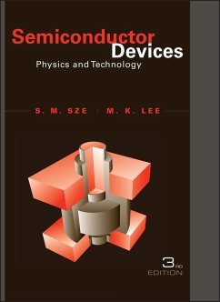
Semiconductor Devices
Physics and Technology
Simon M. Sze (Inc. Bell Laboratories), Ming-Kwei Lee (PRC National Sun-Yat Sen University)
Semiconductor Devices
Physics and Technology
- Gebundenes Buch
- Merkliste
- Auf die Merkliste
- Bewerten Bewerten
- Teilen
- Produkt teilen
- Produkterinnerung
- Produkterinnerung
Covers all key semiconductor devices with up-to-date information and easy-to-understand descriptions. Each chapter is presented in a logical manner enabling students to learn all important devices from a single source. Covers historical developments of devices and technology in the last 100 years.
Andere Kunden interessierten sich auch für
![Advanced Ultra Low-Power Semiconductor Devices Advanced Ultra Low-Power Semiconductor Devices]() Advanced Ultra Low-Power Semiconductor Devices192,99 €
Advanced Ultra Low-Power Semiconductor Devices192,99 €![Semiconductor Physics and Devices Semiconductor Physics and Devices]() Donald A. NeamenSemiconductor Physics and Devices265,99 €
Donald A. NeamenSemiconductor Physics and Devices265,99 €![The Future of Semiconductor Oxides in Next-Generation Solar Cells The Future of Semiconductor Oxides in Next-Generation Solar Cells]() The Future of Semiconductor Oxides in Next-Generation Solar Cells190,99 €
The Future of Semiconductor Oxides in Next-Generation Solar Cells190,99 €![Introduction to Semiconductor Materials and Devices Introduction to Semiconductor Materials and Devices]() M. S. Tyagi (Indian Institute of Technology, Kanpur, India)Introduction to Semiconductor Materials and Devices246,99 €
M. S. Tyagi (Indian Institute of Technology, Kanpur, India)Introduction to Semiconductor Materials and Devices246,99 €![Making a Semiconductor Superpower Making a Semiconductor Superpower]() Dong-Won KimMaking a Semiconductor Superpower64,99 €
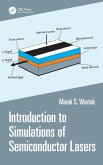
Dong-Won KimMaking a Semiconductor Superpower64,99 €![Introduction to Simulations of Semiconductor Lasers Introduction to Simulations of Semiconductor Lasers]() Marek WartakIntroduction to Simulations of Semiconductor Lasers116,99 €
Marek WartakIntroduction to Simulations of Semiconductor Lasers116,99 €![Transition Metal Oxide Thin Film-Based Chromogenics and Devices Transition Metal Oxide Thin Film-Based Chromogenics and Devices]() Pandurang AshritTransition Metal Oxide Thin Film-Based Chromogenics and Devices199,99 €
Pandurang AshritTransition Metal Oxide Thin Film-Based Chromogenics and Devices199,99 €-
-
-
Covers all key semiconductor devices with up-to-date information and easy-to-understand descriptions. Each chapter is presented in a logical manner enabling students to learn all important devices from a single source. Covers historical developments of devices and technology in the last 100 years.
Hinweis: Dieser Artikel kann nur an eine deutsche Lieferadresse ausgeliefert werden.
Hinweis: Dieser Artikel kann nur an eine deutsche Lieferadresse ausgeliefert werden.
Produktdetails
- Produktdetails
- Verlag: John Wiley & Sons Inc
- 3 ed
- Seitenzahl: 592
- Erscheinungstermin: 15. Mai 2012
- Englisch
- Abmessung: 269mm x 212mm x 25mm
- Gewicht: 1166g
- ISBN-13: 9780470537947
- ISBN-10: 0470537949
- Artikelnr.: 32304325
- Herstellerkennzeichnung
- Libri GmbH
- Europaallee 1
- 36244 Bad Hersfeld
- gpsr@libri.de
S. M. Sze, PhD, is UMC Chair Professor in the Electronics Engineering Department at the National Chiao Tung University. His previous books include Semiconductor Devices; Physics of Semiconductor Devices, Second Edition; High-Speed Semiconductor Devices; and Semiconductor Sensors, all available from Wiley. Ming-Kwei Lee is the author of Semiconductor Devices: Physics and Technology, 3rd Edition, published by Wiley.
Preface vii
Acknowledgments ix
Chapter 0 Introduction 1
0.1 Semiconductor Devices 1
0.2 Semiconductor Technology 6
Summary 12
PART I SEMICONDUCTOR PHYSICS
Chapter 1 Energy Bands and Carrier Concentration in Thermal Equilibrium 15
1.1 Semiconductor Materials 15
1.2 Basic Crystal Structures 17
1.3 Valence Bonds 22
1.4 Energy Bands 23
1.5 Intrinsic Carrier Concentration 29
1.6 Donors and Acceptors 34
Summary 40
Chapter 2 Carrier Transport Phenomena 43
2.1 Carrier Drift 43
2.2 Carrier Diffusion 53
2.3 Generation and Recombination Processes 56
2.4 Continuity Equation 62
2.5 Thermionic Emission Process 68
2.6 Tunneling Process 69
2.7 Space-Charge Effect 71
2.8 High-Field Effects 73
Summary 77
PART II SEMICONDUCTOR DEVICES
Chapter 3 p-n Junction 82
3.1 Thermal Equilibrium Condition 83
3.2 Depletion Region 87
3.3 Depletion Capacitance 95
3.4 Current-Voltage Characteristics 99
3.5 Charge Storage and Transient Behavior 108
3.6 Junction Breakdown 111
3.7 Heterojunction 117
Summary 120
Chapter 4 Bipolar Transistors and Related Devices 123
4.1 Transistor Action 124
4.2 Static Characteristics of Bipolar Transistors 129
4.3 Frequency Response and Switching of Bipolar Transistors 137
4.4 Nonideal Effects 142
4.5 Heterojunction Bipolar Transistors 146
4.6 Thyristors and Related Power Devices 149
Summary 155
Chapter 5 MOS Capacitor and MOSFET 160
5.1 Ideal MOS Capacitor 160
5.2 SiO2-Si MOS Capacitor 169
5.3 Carrier Transport in MOS Capacitors 174
5.4 Charge-Coupled Devices 177
5.5 MOSFET Fundamentals 180
Summary 192
Chapter 6 Advanced MOSFET and Related Devices 195
6.1 MOSFET Scaling 195
6.2 CMOS and BiCMOS 205
6.3 MOSFET on Insulator 210
6.4 MOS Memory Structures 214
6.5 Power MOSFET 223
Summary 224
Chapter 7 MESFET and Related Devices 228
7.1 Metal-Semiconductor Contacts 229
7.2 MESFET 240
7.3 MODFET 249
Summary 255
Chapter 8 Microwave Diodes; Quantum-Effect and Hot-Electron Devices 258
8.1 Microwave Frequency Bands 259
8.2 Tunnel Diode 260
8.3 IMPATT Diode 260
8.4 Transferred-Electron Devices 265
8.5 Quantum-Effect Devices 269
8.6 Hot-Electron Devices 274
Summary 277
Chapter 9 Light Emitting Diodes and Lasers 280
9.1 Radiative Transitions and Optical Absorption 280
9.2 Light-Emitting Diodes 286
9.3 Various Light-Emitting Diodes 291
9.4 Semiconductor Lasers 302
Summary 319
Chapter 10 Photodetectors and Solar Cells 323
10.1 Photodetectors 323
10.2 Solar Cells 336
10.3 Silicon and Compound-Semiconductor Solar Cells 343
10.4 Third-Generation Solar Cells 348
10.5 Optical Concentration 352
Summary 352
PART III SEMICONDUCTOR TECHNOLOGY
Chapter 11 Crystal Growth and Epitaxy 357
11.1 Silicon Crystal Growth from the Melt 357
11.2 Silicon Float-Zone Proces 363
11.3 GaAs Grystal-Growth Techniques 367
11.4 Material Characterization 370
11.5 Epitaxial-Growth Techniques 377
11.6 Structures and Defects in Epitaxial Layers 384
Summary 388
Chapter 12 Film Formation 392
12.1 Thermal Oxidation 392
12.2 Chemical Vapor Deposition of Dielectrics 400
12.3 Chemical Vapor Deposition of Polysilicon 409
12.4 Atom Layer Deposition 412
12.5 Metallization 414
Summary 425
Chapter 13 Lithography and Etching 428
13.1 Optical Lithography 428
13.2 Next-Generation Lithographic Methods 441
13.3 Wet Chemical Etching 447
13.4 Dry Etching 450
Summary 462
Chapter 14 Impurity Doping 466
14.1 Basic Diffusion Process 467
14.2 Extrinsic Diffusion 476
14.3 Diffusion-Related Processes 480
14.4 Range of Implanted Ions 483
14.5 Implant Damage and Annealing 490
14.6 Implantation-Related Processes 495
Summary 501
Chapter 15 Integrated Devices 505
15.1 Passive Components 507
15.2 Bipolar Technology 511
15.3 MOSFET Technology 516
15.4 MESFET Technology 529
15.5 Challenges for Nanoelectronics 532
Summary 537
APPENDIX A List of Symbols 541
APPENDIX B International Systems of Units (SI Units) 543
APPENDIX C Unit Prefixes 544
APPENDIX D Greek Alphabet 545
APPENDIX E Physical Constants 546
APPENDIX F Properties of Important Element and Binary Compound
Semiconductors at 300 K 547
APPENDIX G Properties of Si and GaAs at 300 K 548
APPENDIX H Derivation of the Density of States in a Semiconductor 549
APPENDIX I Derivation of Recombination Rate for Indirect Recombination 553
APPENDIX J Calculation of the Transmission Coefficient for a Symmetric
Resonant-Tunneling Diode 555
APPENDIX K Basic Kinetic Theory of Gases 557
APPENDIX L Answers to Selected Problems 559
Photo Credits 563
Index 565

