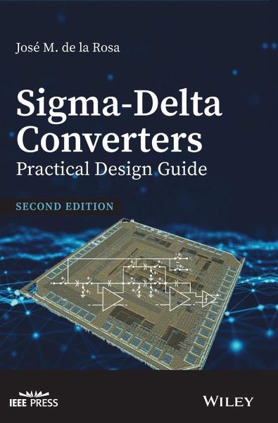
Jose M de la Rosa
Sigma-Delta Converters: Practical Design Guide
Jose M de la Rosa
Sigma-Delta Converters: Practical Design Guide
- Gebundenes Buch
- Merkliste
- Auf die Merkliste
- Bewerten Bewerten
- Teilen
- Produkt teilen
- Produkterinnerung
- Produkterinnerung
Thoroughly Revised and Expanded to Help Readers Systematically Increase Their Knowledge and Insight About Sigma-Delta Modulators Sigma-Delta Modulators (Ms) have become one of the best choices for the implementation of analog/digital interfaces of electronic systems integrated in CMOS technologies. Compared to other kinds of Analog-to-Digital Converters (ADCs), Ms cover one of the widest conversion regions of the resolution-versus-bandwidth plane, being the most efficient solution to digitize signals in an increasing number of applications, which span from high-resolution low-bandwidth digital…mehr
Andere Kunden interessierten sich auch für
- Robert H.M. van VeldhovenRobust SIGMA Delta Converters117,99 €
- Rocío Río FernándezCMOS Cascade Sigma-Delta Modulators for Sensors and Telecom192,99 €
- Erwin JanssenLook-Ahead Based Sigma-Delta Modulation110,99 €
- Robert H.M. van VeldhovenRobust Sigma Delta Converters110,99 €
- Erwin JanssenLook-Ahead Based Sigma-Delta Modulation189,99 €
- Mücahit KozakOversampled Delta-Sigma Modulators94,99 €
- Søren HeinSigma Delta Modulators125,99 €
-
-
-
Thoroughly Revised and Expanded to Help Readers Systematically Increase Their Knowledge and Insight About Sigma-Delta Modulators Sigma-Delta Modulators (Ms) have become one of the best choices for the implementation of analog/digital interfaces of electronic systems integrated in CMOS technologies. Compared to other kinds of Analog-to-Digital Converters (ADCs), Ms cover one of the widest conversion regions of the resolution-versus-bandwidth plane, being the most efficient solution to digitize signals in an increasing number of applications, which span from high-resolution low-bandwidth digital audio, sensor interfaces, and instrumentation, to ultra-low power biomedical systems and medium-resolution broadband wireless communications. Following the spirit of its first edition, Sigma-Delta Converters: Practical Design Guide, 2nd Edition takes a comprehensive look at Ms, their diverse types of architectures, circuit techniques, analysis synthesis methods, and CAD tools, as well as their practical design considerations. It compiles and updates the current research reported on the topic, and explains the multiple trade-offs involved in the whole design flow of Ms--from specifications to chip implementation and characterization. The book follows atop-downapproach in order to provide readers with the necessary understanding about recent advances, trends, and challenges in state-of-the-art Ms. It places more emphasis on two key points, which were not treated so deeply in the first edition: * It includes a more detailed explanation of Ms implemented using Continuous-Time (CT) circuits, going from system-level synthesis to practical circuit limitations. * It provides more practical case studies and applications, as well as a deeper description of the synthesis methodologies and CAD tools employed in the design of converters. Sigma-Delta Converters: Practical Design Guide, 2nd Editionserves as an excellent textbook for undergraduate and graduate students in electrical engineering as well as design engineers working on data converters, who are looking for a uniform and self-contained reference in this hot topic. With this goal in mind, and based on the feedback received from readers, the contents have been revised and structured to make this new edition a unique monograph written in a didactical, pedagogical, and intuitive style.
Hinweis: Dieser Artikel kann nur an eine deutsche Lieferadresse ausgeliefert werden.
Produktdetails
- Produktdetails
- Verlag: Wiley
- 2nd edition
- Seitenzahl: 576
- Erscheinungstermin: 5. November 2018
- Englisch
- Abmessung: 250mm x 175mm x 35mm
- Gewicht: 1142g
- ISBN-13: 9781119275787
- ISBN-10: 1119275784
- Artikelnr.: 53690008
- Verlag: Wiley
- 2nd edition
- Seitenzahl: 576
- Erscheinungstermin: 5. November 2018
- Englisch
- Abmessung: 250mm x 175mm x 35mm
- Gewicht: 1142g
- ISBN-13: 9781119275787
- ISBN-10: 1119275784
- Artikelnr.: 53690008
José M. de la Rosa is a Professor at the Institute of Microelectronics of Seville, IMSE-CNM (CSIC, University of Seville, Spain). His main research interests are in the field of analog and mixed-signal integrated circuits, especially high-performance sigma-delta converters. He has worked in a number of international research and industrial projects and has co-authored over 200 peer-reviewed conference and journal papers dealing with sigma-delta ADCs. He served as Associated Editor of the IEEE Transactions on Circuits and Systems ? I: Regular Papers, as Deputy Editor in Chief of the IEEE Transactions on Circuits and Systems ? II: Express Briefs, and as Distinguished Lecturer of the IEEE Circuits and Systems Society.
Preface xix Acknowledgements xxv List of Abbreviations xxvii 1 Introduction to
Modulators: Fundamentals, Basic Architecture and Performance Metrics 1 1.1 Basics of Analog-to-Digital Conversion 2 1.1.1 Sampling 3 1.1.2 Quantization 4 1.1.3 Quantization White Noise Model 5 1.1.4 Noise Shaping 8 1.2 Sigma-Delta Modulation 9 1.2.1 From Noise-shaped Systems to
Modulators 10 1.2.2 Performance Metrics of
Ms 11 1.3 The First-order
Modulator 13 1.4 Performance Enhancement and Taxonomy of
Ms 16 1.4.1
M System-level Design Parameters and Strategies 17 1.4.2 Classification of
Ms 18 1.5 Putting All The Pieces Together: From
Ms to
ADCs 19 1.5.1 Some Words about
Decimators 20 1.6
DACs 22 1.6.1 System Design Trade-offs and Signal Processing in
DACs 22 1.6.2 Implementation of Digital
Ms used in DACs 24 1.7 Summary 25 References 26 2 Taxonomy of
Architectures 29 2.1 Second-order
Modulators 30 2.1.1 Alternative Representations of Second-order
Ms 31 2.1.2 Second-Order
M with Unity STF 34 2.2 High-order Single-loop
Ms 35 2.3 Cascade
Modulators 39 2.3.1 SMASH
M Architectures 46 2.4 Multi-bit
Modulators 49 2.4.1 Influence of Multi-bit DAC Errors 49 2.4.2 Dynamic Element Matching Techniques 50 2.4.3 Dual Quantization 53 2.4.3.1 Dual-quantization Single-loop
Ms 53 2.4.3.2 Dual-quantization Cascade
Ms 54 2.5 Band-pass
Modulators 55 2.5.1 Quadrature BP-
Ms 56 2.5.2 The z
z2 LP-BP Transformation 58 2.5.3 BP-
Ms with Optimized NTF 58 2.5.4 Time-interleaved and Polyphase BP-
Ms 61 2.6 Continuous-time
Modulators: Architecture and Basic Concepts 64 2.6.1 An Intuitive Analysis of CT-
Ms 66 2.6.2 Some Words about Alias Rejection in CT-
Ms 69 2.7 DT-CT Transformation of
Ms 70 2.7.1 The Impulse-invariant Transformation 70 2.7.2 DT-CT Transformation of a Second-order
M 72 2.8 Direct Synthesis of CT-
Ms 74 2.9 Summary 76 References 76 3 Circuit Errors in Switched-capacitor
Modulators 83 3.1 Overview of Nonidealities in Switched-capacitor
Modulators 84 3.2 Finite Amplifier Gain in SC-
Ms 86 3.3 Capacitor Mismatch in SC-
Ms 90 3.4 Integrator Settling Error in SC-
Ms 91 3.4.1 Behavioral Model for the Integrator Settling 91 3.4.2 Linear Effect of Finite Amplifier Gain-Bandwidth Product 95 3.4.3 Nonlinear Effect of Finite Amplifier Slew Rate 98 3.4.4 Effect of Finite Switch On-resistance 100 3.5 Circuit Noise in SC-
Ms 101 3.6 Clock Jitter in SC-
Ms 105 3.7 Sources of Distortion in SC-
Ms 107 3.7.1 Nonlinear Amplifier Gain 107 3.7.2 Nonlinear Switch On-Resistance 109 3.8 Case Study: High-level Sizing of a
M 111 3.8.1 Ideal Modulator Performance 111 3.8.2 Noise Leakages 112 3.8.3 Circuit Noise 115 3.8.4 Settling Error 116 3.8.5 Overall High-Level Sizing and Noise Budget 117 3.9 Summary 119 References 119 4 Circuit Errors and Compensation Techniques in Continuous-time
Modulators 123 4.1 Overview of Nonidealities in Continuous-time
Modulators 123 4.2 CT Integrators and Resonators 124 4.3 Finite Amplifier Gain in CT-
Ms 126 4.4 Time-constant Error in CT-
Ms 128 4.5 Finite Integrator Dynamics in CT-
Ms 130 4.5.1 Effect of Finite Gain-Bandwidth Product on CT-
Ms 131 4.5.2 Effect of Finite Slew Rate on CT-
Ms 133 4.6 Sources of Distortion in CT-
Ms 134 4.6.1 Nonlinearities in the Front-end Integrator 134 4.6.2 Intersymbol Interference in the Feedback DAC 136 4.7 Circuit Noise in CT-
Ms 137 4.7.1 Noise Analysis Considering NRZ Feedback DACs 137 4.7.2 Noise Analysis Considering SC Feedback DACs 139 4.8 Clock Jitter in CT-
Ms 140 4.8.1 Jitter in Return-to-zero DACs 141 4.8.2 Jitter in Non-return-to-zero DACs 142 4.8.3 Jitter in Switched-capacitor DACs 144 4.8.4 Lingering Effect of Clock Jitter Error 145 4.8.5 Reducing the Effect of Clock Jitter with FIR and Sine-shaped DACs 147 4.9 Excess Loop Delay in CT-
Ms 149 4.9.1 Intuitive Analysis of ELD 149 4.9.2 Analysis of ELD based on Impulse-invariant DT-CT Transformation 151 4.9.3 Alternative ELD Compensation Techniques 154 4.10 Quantizer Metastability in CT-
Ms 155 4.11 Summary 159 References 160 5 Behavioral Modeling and High-level Simulation 165 5.1 Systematic Design Methodology of
Modulators 165 5.1.1 System Partitioning and Abstraction Levels 167 5.1.2 Sizing Process 167 5.2 Simulation Approaches for the High-level Evaluation of
Ms 169 5.2.1 Alternatives to Transistor-level Simulation 169 5.2.2 Event-driven Behavioral Simulation Technique 171 5.2.3 Programming Languages and Behavioral Modeling Platforms 172 5.3 Implementing
M Behavioral Models 173 5.3.1 From Circuit Analysis to Computational Algorithms 173 5.3.2 Time-domain versus Frequency-domain Behavioral Models 175 5.3.3 Implementing Time-domain Behavioral Models in MATLAB 178 5.3.4 Building Time-domain Behavioral Models as SIMULINK C-MEX S-functions 182 5.4 Efficient Behavioral Modeling of
M Building Blocks using C-MEX S-functions 188 5.4.1 Modeling of SC Integrators using S-functions 188 5.4.1.1 Capacitor Mismatch and Nonlinearity 190 5.4.1.2 Input-referred Thermal Noise 191 5.4.1.3 Switch On-resistance Dynamics 194 5.4.1.4 Incomplete Settling Error 197 5.4.2 Modeling of CT Integrators using S-functions 200 5.4.2.1 Single-pole Gm-C Model 200 5.4.2.2 Two-pole Dynamics Model 201 5.4.2.3 Modeling Transconductors as S-functions 203 5.4.3 Behavioral Modeling of Quantizers using S-functions 205 5.4.3.1 Modeling Multi-level ADCs as S-functions 205 5.4.3.2 Modeling Multi-level DACs as S-functions 207 5.5 SIMSIDES: A SIMULINK-based Behavioral Simulator for
Ms 209 5.5.1 Model Libraries Included in SIMSIDES 210 5.5.2 Structure of SIMSIDES and its User Interface 211 5.5.2.1 Creating a New
M Block Diagram 212 5.5.2.2 Setting Model Parameters 215 5.5.2.3 Simulation Analyses 215 5.6 Using SIMSIDES for High-level Sizing and Verification of
Ms 216 5.6.1 SC Second-order Single-Bit
M 216 5.6.1.1 Effect of Amplifier Finite DC Gain 218 5.6.1.2 Effect of Thermal Noise 218 5.6.1.3 Effect of the Incomplete Settling Error 220 5.6.1.4 Cumulative Effect of All Errors 221 5.6.2 CT Fifth-order Cascade 3-2 Multi-bit
M 224 5.6.2.1 Effect of Nonideal Effects 227 5.6.2.2 High-level Synthesis and Verification 229 5.7 Summary 231 References 231 6 Automated Design and Optimization of
Ms 235 6.1 Architecture Exploration and Selection: Schreier's Toolbox 236 6.1.1 Basic Functions of Schreier's Delta-Sigma Toolbox 236 6.1.2 Synthesis of a Fourth-order CRFF LP/BP SC-
M with Tunable Notch 238 6.1.3 Synthesis of a Fourth-order BP CT-
M with Tunable Notch 240 6.2 Optimization-based High-level Synthesis of
Modulators 245 6.2.1 Combining Behavioral Simulation and Optimization 246 6.2.2 Using Simulated Annealing as Optimization Engine 247 6.2.3 Combining SIMSIDES with MATLAB Optimizers 253 6.3 Lifting Method and Hardware Acceleration to Optimize CT-
Ms 255 6.3.1 Hardware Emulation of CT-
Ms on an FPGA 257 6.3.2 GPU-accelerated Computing of CT-
Ms 258 6.4 Using Multi-objective Evolutionary Algorithms to Optimize
Ms 259 6.4.1 Combining MOEA with SIMSIDES 261 6.4.2 Applying MOEA and SIMSIDES to the Synthesis of CT-
Ms 262 6.5 Summary 269 References 269 7 Electrical Design of
Ms: From Systems to Circuits 271 7.1 Macromodeling
Ms 272 7.1.1 SC Integrator Macromodel 272 7.1.1.1 Switch Macromodel 272 7.1.1.2 OTA Macromodel 274 7.1.2 CT Integrator Macromodel 274 7.1.2.1 Active-RC Integrators 274 7.1.2.2 Gm-C Integrators 274 7.1.3 Nonlinear OTA Transconductor 275 7.1.4 Embedded Flash ADC Macromodel 276 7.1.5 Feedback DAC Macromodel 277 7.2 Examples of
M Macromodels 279 7.2.1 SC Second-order Example 279 7.2.2 Second-order Active-RC
M 283 7.3 Including Noise in Transient Electrical Simulations of
Ms 286 7.3.1 Generating and Injecting Noise Data Sequences in HSPICE 287 7.3.2 Analyzing the Impact of the Main Noise Sources in SC Integrators 289 7.3.3 Generating and Injecting Flicker Noise Sources in Electrical Simulations 289 7.3.4 Test Bench to Include Noise in the Simulation of
Ms 293 7.4 Processing
M Output Results of Electrical Simulations 294 7.5 Summary 298 References 298 8 Design Considerations of
M Subcircuits 301 8.1 Design Considerations of CMOS Switches 302 8.1.1 Trade-Off Between Ron and the CMOS Switch Drain/Source Parasitic Capacitances 302 8.1.2 Characterizing the Nonlinear Behavior of Ron 302 8.1.3 Influence of Technology Downscaling on the Design of Switches 304 8.1.4 Evaluating Harmonic Distortion due to CMOS Switches 305 8.2 Design Considerations of Operational Amplifiers 308 8.2.1 Typical Amplifier Topologies 309 8.2.2 Common-mode Feedback Networks 311 8.2.3 Characterization of the Amplifier in AC 313 8.2.4 Characterization of the Amplifier in DC 313 8.2.5 Characterization of the Amplifier Gain Nonlinearity 316 8.3 Design Considerations of Transconductors 317 8.3.1 Highly Linear Front-end Transconductor 318 8.3.2 Loop-filter Transconductors 320 8.3.3 Widely Programmable Transconductors 323 8.4 Design Considerations of Comparators 324 8.4.1 Regenerative Latch-based Comparators 325 8.4.2 Design Guidelines of Comparators 327 8.4.3 Characterization of Offset and Hysteresis Based on the Input-ramp Method 328 8.4.4 Characterization of Offset and Hysteresis Based on the Bisectional Method 328 8.4.5 Characterizing the Comparison Time 330 8.5 Design Considerations of Current-Steering DACs 332 8.5.1 Fundamentals and Basic Concepts of CS DACs 333 8.5.2 Practical Realization of CS DACs 333 8.5.3 Current Cell Circuits, Error Limitations, and Design Criteria 336 8.5.4 CS 4-bit DAC Example 336 8.6 Summary 338 References 338 9 Practical Realization of
Ms: From Circuits to Chips 341 9.1 Auxiliary
M Building Blocks 341 9.1.1 Clock-phase Generators 342 9.1.1.1 Phase Generation 342 9.1.1.2 Phase Buffering 342 9.1.1.3 Phase Distribution 344 9.1.2 Generation of Common-mode Voltage, Reference Voltage, and Bias Currents 345 9.1.2.1 Bandgap Circuit 345 9.1.2.2 Reference Voltage Generator 345 9.1.2.3 Master Bias Current Generator 346 9.1.2.4 Common-mode Voltage Generator 346 9.1.3 Additional Digital Logic 347 9.2 Layout Design, Floorplanning, and Practical Issues 348 9.2.1 Layout Floorplanning 348 9.2.1.1 Divide Layout into Different Parts or Regions 348 9.2.1.2 Shield Sensitive
M Analog Subcircuits from Switching Noise 349 9.2.1.3 Buses to Distribute Signals Shared by Different
M Parts 349 9.2.1.4 Be Obsessive about Layout Symmetry and Details of Analog Parts 349 9.2.2 I/O Pad Ring 350 9.2.3 Importance of Layout Verification and Catastrophic Failure 350 9.3 Chip Package, Test PCB, and Experimental Setup 354 9.3.1 Bonding Diagram and Package 354 9.3.2 Test PCB 355 9.4 Experimental Test Set-Up 355 9.4.1 Planning the Type and Number of Instruments Needed 357 9.4.2 Connecting Lab Instruments 357 9.4.3 Measurement Set-Up Example 358 9.5
M Design Examples and Case Studies 359 9.5.1 Programmable-gain
Ms for High Dynamic Range Sensor Interfaces 360 9.5.1.1 Main Design Criteria and Performance Limitations 361 9.5.1.2 SC Realization with Programmable Gain and Double Sampling 362 9.5.1.3 Influence of Chopper Frequency on Flicker Noise 362 9.5.2 Reconfigurable SC-
Ms for Multi-standard Direct Conversion Receivers 364 9.5.2.1 Power-scaling Circuit Techniques 367 9.5.2.2 Experimental Results 368 9.5.3 Using Widely-programmable Gm-LC BP-
Ms for RF Digitizers 368 9.5.3.1 Application Scenario 371 9.5.3.2 Gm-LC BP-
M High-level Sizing 371 9.5.3.3 BP CT-
M Loop-Filter Reconfiguration Techniques 375 9.5.3.4 Embedded 4-bit Quantizer with Calibration 378 9.5.3.5 Biasing, Digital Control Programmability and Testability 382 9.6 Summary 385 References 386 10 Frontiers, Trends and Challenges: Towards Next-generation
Modulators 389 10.1 State-of-the-Art ADCs: Nyquist-rate versus
Converters 390 10.1.1 Conversion Energy 391 10.1.2 Figures of Merit 392 10.2 Comparison of Different Categories of
ADCs 393 10.2.1 Aperture Plot of
Ms 406 10.2.2 Energy Plot of
Ms 407 10.3 Empirical and Statistical Analysis of State-of-the-Art
Ms 408 10.3.1 SC versus CT
Ms 408 10.3.2 Technology used in State-of-the-Art
Ms 410 10.3.3 Single-Loop versus Cascade
Ms 410 10.3.4 Single-bit versus Multi-bit
Ms 411 10.3.5 Low-pass versus Band-pass
Ms 413 10.3.6 Emerging
M Techniques 415 10.4 Gigahertz-range
Ms for RF-to-digital Conversion 415 10.5 Enhanced Cascade
Ms 418 10.5.1 SMASH CT-
Ms 418 10.5.2 Two-stage 0-L MASH 419 10.5.3 Stage-sharing Cascade
Ms 420 10.5.4 Multi-rate and Hybrid CT/DT
Ms 420 10.5.4.1 Upsampling Cascade MR-
Ms 421 10.5.4.2 Downsampling Hybrid CT/DT Cascade MR-
Ms 422 10.6 Power-efficient
M Loop-filter Techniques 423 10.6.1 Inverter-based
Ms 423 10.6.2 Hybrid Active/Passive and Amplifier-less
Ms 424 10.6.3 Power-efficient Amplifier Techniques 426 10.7 Hybrid
M/Nyquist-rate ADCs 428 10.7.1 Multi-bit
M Quantizers based on Nyquist-rate ADCs 428 10.7.2 Incremental
ADCs 429 10.8 Time-based
ADCs 431 10.8.1
Ms with VCO/PWM-based Quantization 432 10.8.2 Scaling-friendly Mostly-digital
Ms 433 10.8.3 GRO-based
Ms 434 10.9 DAC Techniques for High-performance CT-
Ms 436 10.10 Classification of State-of-the-Art References 437 10.11 Summary and Conclusions 437 References 438 A State-space Analysis of Clock Jitter in CT-
Ms 463 A.1 State-space Representation of NTF (z) 463 A.2 Expectation Value of (
qn)2 465 A.3 In-band Noise Power due to Clock Jitter 466 References 467 B SIMSIDES User Guide 469 B.1 Getting Started: Installing and Running SIMSIDES 470 B.2 Building and Editing
M Architectures in SIMSIDES 470 B.3 Analyzing
Ms in SIMSIDES 473 B.3.1 Node Spectrum Analysis 474 B.3.2 Integrated Power Noise 474 B.3.3 SNR/SNDR 475 B.3.4 Harmonic Distortion 475 B.3.5 Integral and Differential Non-Linearity 477 B.3.6 Multi-tone Power Ratio 477 B.3.7 Histogram 478 B.3.8 Parametric Analysis 478 B.3.9 Monte Carlo Analysis 479 B.4 Optimization Interface 480 B.5 Tutorial Example: Using SIMSIDES to Model and Analyze
Ms 482 B.5.1 Creating the Cascade 2-1
M Block Diagram in SIMSIDES 482 B.5.2 Setting Model Parameters 482 B.5.3 Computing the Output Spectrum 484 B.5.4 SNR versus Input Amplitude Level 486 B.5.5 Parametric Analysis Considering Only One Parameter 487 B.5.6 Parametric Analysis Considering Two Parameters 488 B.5.7 Computing Histograms 489 B.6 Getting Help 489 C SIMSIDES Block Libraries and Models 491 C.1 Overview of SIMSIDES Libraries 491 C.2 Ideal Libraries 492 C.2.1 Ideal Integrators 492 C.2.1.1 Building-block Model Purpose and Description 492 C.2.1.2 Model Parameters 493 C.2.2 Ideal Resonators 493 C.2.2.1 Ideal_LD_Resonator 493 C.2.2.2 Ideal_FE_Resonator 493 C.2.2.3 Ideal_CT_Resonator 493 C.2.3 Ideal Quantizers 494 C.2.3.1 Ideal_Comparator 494 C.2.3.2 Ideal_Comparator_for_SI 495 C.2.3.3 Ideal_Multibit_Quantizer 495 C.2.3.4 Ideal_Multibit_Quantizer_for_SI 496 C.2.3.5 Ideal_Multibit_Quantizer_levels 496 C.2.3.6 Ideal_Multibit_Quantizer_levels_SD2 496 C.2.3.7 Ideal_Sampler 496 C.2.4 Ideal D/A Converters 496 C.2.4.1 Ideal_DAC_for_SI 496 C.2.4.2 Ideal_DAC_dig_level_SD2 497 C.3 Real SC Building-Block Libraries 497 C.3.1 Real SC Integrators 497 C.3.2 Real SC Resonators 501 C.4 Real SI Building-Block Libraries 503 C.4.1 Real SI Integrators 503 C.4.2 Real SI Resonators 505 C.4.3 SI Errors and Model Parameters 506 C.4.3.1 Basic_SI_FE(LD)_Integrator and Basic_SI_FE(LD)_Resonator 506 C.4.3.2 SI_FE(LD)_Int_Finite_Conductance 507 C.4.3.3 SI_FE(LD)_Int_Finite_Conductance & Settling & ChargeInjection 508 C.5 Real CT Building-Block Libraries 508 C.5.1 Real CT Integrators 508 C.5.1.1 Model Parameters used in Transconductors and Gm-C Integrator Building Blocks 511 C.5.1.2 Gm-MC Integrators 511 C.5.1.3 Active-RC Integrators 512 C.5.1.4 MOSFET-C Integrators 513 C.5.2 Real CT Resonators 513 C.5.2.1 Gm-C Resonators 514 C.5.2.2 Gm-LC Resonators 517 C.6 Real Quantizers & Comparators 517 C.7 Real D/A Converters 518 C.8 Auxiliary Blocks 519 Index 523