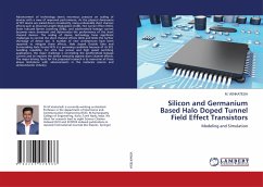
Silicon and Germanium Based Halo Doped Tunnel Field Effect Transistors
Modeling and Simulation
Versandkostenfrei!
Versandfertig in 6-10 Tagen
51,99 €
inkl. MwSt.

PAYBACK Punkte
26 °P sammeln!
Advancement of technology exerts enormous pressure on scaling of devices with a view of improved performance. As the physical dimensions of FET device are scaled down consistently, many undesirable short channel effects such as Channel Length Modulation (CLM), Hot Carrier Effect (HCE), Drain Induced Barrier Lowering (DIBL), and subthreshold leakage current becomes more dominant and deteriorates the performance of the short channel devices. The scaling of device technology faces significant challenges to control the short channel effects (SCE) and limits the further shrinkage of device size. A ...
Advancement of technology exerts enormous pressure on scaling of devices with a view of improved performance. As the physical dimensions of FET device are scaled down consistently, many undesirable short channel effects such as Channel Length Modulation (CLM), Hot Carrier Effect (HCE), Drain Induced Barrier Lowering (DIBL), and subthreshold leakage current becomes more dominant and deteriorates the performance of the short channel devices. The scaling of device technology faces significant challenges to control the short channel effects (SCE) and limits the further shrinkage of device size. A number of new architectures have been reported to mitigate these effects. Halo doped Double Gate and Surrounding Gate Tunnel FETs is a promising candidate because of its SCE handling capability. For ultra low power and high speed switching applications, the major challenge is controlling the subthreshold leakage current and to improve the device immunity against short channel effects. The major driving force for the proposed research is to overcome all these above limitations with advancements in the materials science and semiconductor industry.


