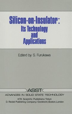
This volume contains papers presented during the US-Japan seminar on "Solid Phase Epitaxy and Interface Kinetics" held in Oiso, Japan, June 20-24, 1983. This seminar was co-sponsored by the National Science Foun dation and Japan Society for the Promotion of Science and co-chaired by Professor S. Furukawa, Tokyo Insitute of Technology, and Professor J. W. Mayer, Cornell University. Extensive topics such as solid phase epitaxy, growth mechanisms and interface kinetics, silicon-on-insulator structures, silicide-on-Si sturctures, novel nanometer and layered devices, and so on were discussed and more than 50 papers were presented. Most papers were original ones with brief reviews added for the convenience of the readers at the editor's request. The editor classified these papers into two groups and compiled two volumes; "Silicon-on-Insulator (SOl): Its Technology and Applications" and "Layered Structures and Interface Kinetics: Their Technology and Ap plications". This volume mainly contains the papers related to epitaxial growth of metal, insulator and semiconductor films, growth mechanisms, interface kinetics, properties and applications of silicide films, and novel nanometer and layered devices. These papers offer basic properties of the layered structures and possibility of various applications of the structures to present and future semiconductor devices. The editor is indebted to our fellow contributors who agreed to par take in publishing the proceedings of the seminar, to Japanese principal par ticipants of the seminar for encouraging him to have the seminar and to compile these volumes, to Professor H. Ishiwara for his secretarial work throughout the seminar and the publication.
Hinweis: Dieser Artikel kann nur an eine deutsche Lieferadresse ausgeliefert werden.
Hinweis: Dieser Artikel kann nur an eine deutsche Lieferadresse ausgeliefert werden.

