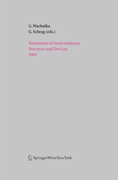
Gerhard Wachutka / Gabriele Schrag (eds.)
Simulation of Semiconductor Processes and Devices 2004
Herausgegeben:Wachutka, Gerhard; Schrag, Gabriele
Gerhard Wachutka / Gabriele Schrag (eds.)
Simulation of Semiconductor Processes and Devices 2004
Herausgegeben:Wachutka, Gerhard; Schrag, Gabriele
- Gebundenes Buch
- Merkliste
- Auf die Merkliste
- Bewerten Bewerten
- Teilen
- Produkt teilen
- Produkterinnerung
- Produkterinnerung
This volume contains the proceedings of the 10th edition of the International Conference on Simulation of Semiconductor Processes and Devices (SISPAD 2004), held in Munich, Germany, on September 2-4, 2004.The conference program included 7 invited plenary lectures and 82 contributed papers for oral or poster presentation, which were carefully selected out of a total of 151 abstracts submitted from 14 countries around the world.Like the previous meetings, SISPAD 2004 provided a world-wide forum for the presentation and discussion of recent advances and developments in the theoretical…mehr
Andere Kunden interessierten sich auch für
![Simulation of Semiconductor Processes and Devices 2004 Simulation of Semiconductor Processes and Devices 2004]() Simulation of Semiconductor Processes and Devices 2004161,99 €
Simulation of Semiconductor Processes and Devices 2004161,99 €![Simulation of Semiconductor Processes and Devices 2007 Simulation of Semiconductor Processes and Devices 2007]() Tibor Grasser / Siegfried Selberherr (eds.)Simulation of Semiconductor Processes and Devices 2007112,99 €
Tibor Grasser / Siegfried Selberherr (eds.)Simulation of Semiconductor Processes and Devices 2007112,99 €![Nitride Semiconductors and Devices Nitride Semiconductors and Devices]() Hadis MorkoçNitride Semiconductors and Devices161,99 €
Hadis MorkoçNitride Semiconductors and Devices161,99 €![Simulation of Semiconductor Processes and Devices 1998 Simulation of Semiconductor Processes and Devices 1998]() MeyerSimulation of Semiconductor Processes and Devices 1998161,99 €
MeyerSimulation of Semiconductor Processes and Devices 1998161,99 €![Semiconductor Device Physics and Design Semiconductor Device Physics and Design]() Umesh MishraSemiconductor Device Physics and Design104,99 €
Umesh MishraSemiconductor Device Physics and Design104,99 €![Science and Technology of Semiconductor-On-Insulator Structures and Devices Operating in a Harsh Environment Science and Technology of Semiconductor-On-Insulator Structures and Devices Operating in a Harsh Environment]() Denis Flandre / Alexei N. Nazarov / Peter L.F. Hemment (eds.)Science and Technology of Semiconductor-On-Insulator Structures and Devices Operating in a Harsh Environment81,99 €
Denis Flandre / Alexei N. Nazarov / Peter L.F. Hemment (eds.)Science and Technology of Semiconductor-On-Insulator Structures and Devices Operating in a Harsh Environment81,99 €![Simulation of Semiconductor Processes and Devices 2001 Simulation of Semiconductor Processes and Devices 2001]() Simulation of Semiconductor Processes and Devices 2001161,99 €
Simulation of Semiconductor Processes and Devices 2001161,99 €-
-
-
This volume contains the proceedings of the 10th edition of the International Conference on Simulation of Semiconductor Processes and Devices (SISPAD 2004), held in Munich, Germany, on September 2-4, 2004.The conference program included 7 invited plenary lectures and 82 contributed papers for oral or poster presentation, which were carefully selected out of a total of 151 abstracts submitted from 14 countries around the world.Like the previous meetings, SISPAD 2004 provided a world-wide forum for the presentation and discussion of recent advances and developments in the theoretical description, physical modeling and numerical simulation and analysis of semiconductor fabrication processes, device operation and system performance. The variety of topics covered by the conference contributions reflects the physical effects and technological problems encountered in consequence of the progressively shrinking device dimensions and the ever-growing complexity in device technology.
Hinweis: Dieser Artikel kann nur an eine deutsche Lieferadresse ausgeliefert werden.
Hinweis: Dieser Artikel kann nur an eine deutsche Lieferadresse ausgeliefert werden.
Produktdetails
- Produktdetails
- Verlag: Springer / Springer Vienna / Springer, Wien
- Artikelnr. des Verlages: 11301585, 978-3-211-22468-7
- 2004
- Seitenzahl: 396
- Erscheinungstermin: 23. August 2004
- Englisch
- Abmessung: 257mm x 170mm x 26mm
- Gewicht: 730g
- ISBN-13: 9783211224687
- ISBN-10: 3211224688
- Artikelnr.: 21568687
- Herstellerkennzeichnung Die Herstellerinformationen sind derzeit nicht verfügbar.
Gerhard Wachutka, Technische Universität München, Germany / Gabriele Schrag, Technische Universität München, Germany
Advanced Transport Models for Sub-Micrometer Devices.- NEMO-ID: the First NEGF-Based TCAD Tool.- The Density-Gradient Correction as a Disguised Pilot Wave of de Broglie.- Full Band and Approximated Solutions of the Schrödinger Equation in Silicon Inversion Layers.- A Hybrid 3D Quantum Mechanical Simulation of FinFETs and Nanowire Devices.- On the Calculation of Quasi-Bound States and Their Impact on Direct Tunneling in CMOS Devices.- Quantum Mechanical Simulation in DG MOSFETs Based on a Tight Binding Green's Function Formalism.- Modeling B Uphill Diffusion in the Presence of Ge.- Ab-initio Calculations To Predict Stress Effects on Boron Solubility in Silicon.- Boron Diffusion in Strained and Strain-Relaxed SiGe.- Modeling Dopant Diffusion in SiGe and SiGeC layers.- Continuum Modeling of Indium To Predict SSR Profiles.- Theoretical Analysis of Stress and Surface Orientation Effects on Inversion Carrier Mobility.- CMOS Circuit Performance Enhancement by Surface Orientation Optimization.- Modeling of Stress Induced Layout Effect on Electrical Characteristics of Advanced MOSFETs.- Hole Mobility Enhancement Modeling and Scaling Study for High Performance Strained Ge Buried Channel PMOSFETs.- Three-Dimensional Characterization and Modelling of Stress Distribution in High-Density DRAM Memory Cells.- Strain Optimization To Reduce Gate Leakage Current in MOS Transistors with Silicon Oxynitride Gate Dielectrics by Use of First-Principles Calculations.- Simulation Study of Simple CMOS-Compatible Thin-SOI Vertical Bipolar Transistors on Thin BOX with an Inversion Collector.- Current Collapse Associated with Surface States in GaN-Based HEMT's. Theoretical/Experimental Investigations.- Implications of Gate Misalignment for Ultra-Narrow Multi-Gate Devices.- Source-Side InjectionModeling by Means of the Spherical-Harmonics Expansion of the BTE.- Investigation of a Novel Tunneling Transistor by MEDICI Simulation.- Optimization of BAW Resonator Performance Using Combined Simulation Techniques.- Simulation of GaN-Based Light-Emitting Devices.- On the Validity of the Relaxation Time Approximation for Macroscopic Transport Models.- A Local Mobility Model for Ultra-Thin DGSOI nMOSFETs.- On the Relationship between Carrier Mobility and Velocity in Sub-50 nm MOSFETs via Calibrated Monte Carlo Simulation.- A Method for Determining the Screening Length of the Coulombic Scattering in Non-Degenerate and Degenerate Semiconductors.- 3D Simulation of Process Effects Limiting FinFET Performance and Scalability.- Full Three-Dimensional Analysis of a Non-Volatile Memory Cell.- Three-Dimensional Simulation of Orientation-Dependent Wet Chemical Etching.- Modeling CVD effects in Atomic Layer Deposition on the Feature Scale.- Defect and Carrier Dynamics in Nanotubes under Electronic Excitations: Time-Dependent Density Functional Approaches.- Three-Dimensional Analysis of Schottky Barrier Carbon Nanotube Field Effect Transistors.- Numerical Performance Analysis of Carbon Nanotube (CNT) Embedded MOSFETs.- Parameter Extraction and Validation of an Electronic and Optical Model for Organic Light-Emitting Devices.- Adaptive Surface Triangulations for 3D Process Simulation.- Anisotropic Laplace Refinement for Three-Dimensional Oxidation Simulation.- Monte Carlo Simulation of Ion Implantation in Silicon-Germanium Alloys.- Comprehensive Understanding of Carrier Mobility in MOSFETs with Oxynitrides and Ultrathin Gate Oxides.- Physics and Modeling of Radiation Effects in Advanced CMOS Technology Nodes.- Very High Performance, Sub-20 nm, Strained Si and SixGe1_x, Hetero-Structure, Center Channel (CC) NMOS and PMOS DGFETs.- Scalability of FinFETs and Unstrained-Si/Strained-Si FDSOI-MOSFETs.- Device Performance in Conventional and Strained Si n-MOSFETs with High-K Gate Stacks.- Understanding the Role of Strain in Si-Ge Devices.- Electro-Thermal Simulations of Strained-Si MOSFETs under ESD Conditions.- Simulation of the Cross-Coupling among Snap Back Devices under Transient High Current Stress.- Simulation of the Failure Mechanism of Power DMOS Transistors under Avalanche Stress.- An Accurate and Comprehensive Soft Error Simulator NISES II.- Impact of Scattering on Random Dopant Induced Current Fluctuations in Decanano MOSFETs.- Analysis of Random Doping and Oxide Thickness Induced Fluctuations in Nanoscale Semiconductor Devices through Poisson-Schrödinger Computations.- Stable Simulation of Impurity Fluctuation for Contact Resistance and Schottky Diodes.- Impact of the Floating Body Effect on Noise in SOI Devices Investigated by Hydrodynamic Simulation.- Examination of Spatial Frequency Dependence of Line Edge Roughness on MOS Device Characteristics.- Simulation of Lithography-Caused Gate Length and Interconnect Linewidth Variational Impact on Circuit Performance in Nanoscale Semiconductor Manufacturing.- Optimization of Recessed and Elevated Suicide Source/Drain Contact Structure Using Physical Compact Resistance Modeling and Simulation in Ultra-Thin Body SOI MOSFETs.- A New Backscattering Model for Nano-MOSFET Compact Modeling.- Fully-Depleted SOI-MOSFET Model for Circuit Simulation and Its Application to 1/f Noise Analysis.- Modeling of Carrier Transport Dynamics at GHz-Frequencies for RF Circuit-Simulation.- SPICE-Compatible Macro Model for Split-Gate Compact NVM Cell with Various Gap Sizes.- SET Accurate Compact Model for SET-MOSFETHybrid Circuit Simulation.- 2D Quantum Mechanical (QM) Charge Model and Its Application to Ballistic Transport of Sub-50 nm Bulk Silicon MOSFETs.- Effective Bohm Quantum Potential for Device Simulators Based on Drift-Diffusion and Energy Transport.- Single Ion and Multi Ion MOSFETs Simulation with Density Gradient Model.- Modeling and Simulation of Combined Thermionic Emission-Tunneling Current through Interfacial Isolation Layer.- Experiments on Minority Carrier Diffusion in Silicon: Contribution of Excitons.- Accurate Temperature Drift Model of MOSFETs Mobility for Analog Circuits.- Accurate Modeling of Lattice Site-Dependent Ionization Level of Impurities in ?-SiC Devices.- Strain Scaling for Ultra Thin Silicon NMOS Devices.- CMOS Scaling Analysis Based on ITRS Roadmap by Three-dimensional Mixed-Mode Device Simulation.- Comparison of Nanoscale Metal-Oxide-Semiconductor Field Effect Transistors.- Numerical Analysis for the Structure Dependence on the Subthreshold Slope of Floating Channel Type SGT(FC-SGT) Flash Memory.- A Monte-Carlo Method for Distribution of Standby Currents and Its Application to DRAM Retention Time.- Optimal Contact Placement in Partially Depleted SOI with Application to Raised Source-Drain Structures.- Simulation of Microstructure Formation during Thin Film Deposition.- Effect of Stress on Pattern-Dependent Oxidation of Silicon Nanostructures.- The Evolution of the Resistance and Current Density during Electromigration.- 3-D Physically-Based Electromigration Simulation in Copper-Low-K Interconnect.- 3D Feature-Scale Simulation of Sputter Etching with Coupling to Equipment Simulation.- Automatic Optimization Algorithm for a Direct 2D and 3D Mesh Generation from the Layout Information.- Genetic Algorithm for Optimization and Calibration inProcess Simulation.- Performance Evaluation of Linear Solvers Employed for Semiconductor Device Simulation.- An Analysis of the Effect of Surrounding Gate Structure on Soft Error Immunity.- Analytical Modeling of Ge and Si Double-Gated (DG) NFETs and the Effect of Process Induced Variations (PIV) on Device Performance.- Proposal of Physics-Based Compact Model for Nanoscale MOSFETs Including the Transition from Drift-Diffusion to Ballistic Transport.- A New Methodology for Efficient and Reliable Large-Signal Analysis of RF Power Devices.- Small-Signal Modeling of RFCMOS.
Advanced Transport Models for Sub-Micrometer Devices.- NEMO-ID: the First NEGF-Based TCAD Tool.- The Density-Gradient Correction as a Disguised Pilot Wave of de Broglie.- Full Band and Approximated Solutions of the Schrödinger Equation in Silicon Inversion Layers.- A Hybrid 3D Quantum Mechanical Simulation of FinFETs and Nanowire Devices.- On the Calculation of Quasi-Bound States and Their Impact on Direct Tunneling in CMOS Devices.- Quantum Mechanical Simulation in DG MOSFETs Based on a Tight Binding Green's Function Formalism.- Modeling B Uphill Diffusion in the Presence of Ge.- Ab-initio Calculations To Predict Stress Effects on Boron Solubility in Silicon.- Boron Diffusion in Strained and Strain-Relaxed SiGe.- Modeling Dopant Diffusion in SiGe and SiGeC layers.- Continuum Modeling of Indium To Predict SSR Profiles.- Theoretical Analysis of Stress and Surface Orientation Effects on Inversion Carrier Mobility.- CMOS Circuit Performance Enhancement by Surface Orientation Optimization.- Modeling of Stress Induced Layout Effect on Electrical Characteristics of Advanced MOSFETs.- Hole Mobility Enhancement Modeling and Scaling Study for High Performance Strained Ge Buried Channel PMOSFETs.- Three-Dimensional Characterization and Modelling of Stress Distribution in High-Density DRAM Memory Cells.- Strain Optimization To Reduce Gate Leakage Current in MOS Transistors with Silicon Oxynitride Gate Dielectrics by Use of First-Principles Calculations.- Simulation Study of Simple CMOS-Compatible Thin-SOI Vertical Bipolar Transistors on Thin BOX with an Inversion Collector.- Current Collapse Associated with Surface States in GaN-Based HEMT's. Theoretical/Experimental Investigations.- Implications of Gate Misalignment for Ultra-Narrow Multi-Gate Devices.- Source-Side InjectionModeling by Means of the Spherical-Harmonics Expansion of the BTE.- Investigation of a Novel Tunneling Transistor by MEDICI Simulation.- Optimization of BAW Resonator Performance Using Combined Simulation Techniques.- Simulation of GaN-Based Light-Emitting Devices.- On the Validity of the Relaxation Time Approximation for Macroscopic Transport Models.- A Local Mobility Model for Ultra-Thin DGSOI nMOSFETs.- On the Relationship between Carrier Mobility and Velocity in Sub-50 nm MOSFETs via Calibrated Monte Carlo Simulation.- A Method for Determining the Screening Length of the Coulombic Scattering in Non-Degenerate and Degenerate Semiconductors.- 3D Simulation of Process Effects Limiting FinFET Performance and Scalability.- Full Three-Dimensional Analysis of a Non-Volatile Memory Cell.- Three-Dimensional Simulation of Orientation-Dependent Wet Chemical Etching.- Modeling CVD effects in Atomic Layer Deposition on the Feature Scale.- Defect and Carrier Dynamics in Nanotubes under Electronic Excitations: Time-Dependent Density Functional Approaches.- Three-Dimensional Analysis of Schottky Barrier Carbon Nanotube Field Effect Transistors.- Numerical Performance Analysis of Carbon Nanotube (CNT) Embedded MOSFETs.- Parameter Extraction and Validation of an Electronic and Optical Model for Organic Light-Emitting Devices.- Adaptive Surface Triangulations for 3D Process Simulation.- Anisotropic Laplace Refinement for Three-Dimensional Oxidation Simulation.- Monte Carlo Simulation of Ion Implantation in Silicon-Germanium Alloys.- Comprehensive Understanding of Carrier Mobility in MOSFETs with Oxynitrides and Ultrathin Gate Oxides.- Physics and Modeling of Radiation Effects in Advanced CMOS Technology Nodes.- Very High Performance, Sub-20 nm, Strained Si and SixGe1_x, Hetero-Structure, Center Channel (CC) NMOS and PMOS DGFETs.- Scalability of FinFETs and Unstrained-Si/Strained-Si FDSOI-MOSFETs.- Device Performance in Conventional and Strained Si n-MOSFETs with High-K Gate Stacks.- Understanding the Role of Strain in Si-Ge Devices.- Electro-Thermal Simulations of Strained-Si MOSFETs under ESD Conditions.- Simulation of the Cross-Coupling among Snap Back Devices under Transient High Current Stress.- Simulation of the Failure Mechanism of Power DMOS Transistors under Avalanche Stress.- An Accurate and Comprehensive Soft Error Simulator NISES II.- Impact of Scattering on Random Dopant Induced Current Fluctuations in Decanano MOSFETs.- Analysis of Random Doping and Oxide Thickness Induced Fluctuations in Nanoscale Semiconductor Devices through Poisson-Schrödinger Computations.- Stable Simulation of Impurity Fluctuation for Contact Resistance and Schottky Diodes.- Impact of the Floating Body Effect on Noise in SOI Devices Investigated by Hydrodynamic Simulation.- Examination of Spatial Frequency Dependence of Line Edge Roughness on MOS Device Characteristics.- Simulation of Lithography-Caused Gate Length and Interconnect Linewidth Variational Impact on Circuit Performance in Nanoscale Semiconductor Manufacturing.- Optimization of Recessed and Elevated Suicide Source/Drain Contact Structure Using Physical Compact Resistance Modeling and Simulation in Ultra-Thin Body SOI MOSFETs.- A New Backscattering Model for Nano-MOSFET Compact Modeling.- Fully-Depleted SOI-MOSFET Model for Circuit Simulation and Its Application to 1/f Noise Analysis.- Modeling of Carrier Transport Dynamics at GHz-Frequencies for RF Circuit-Simulation.- SPICE-Compatible Macro Model for Split-Gate Compact NVM Cell with Various Gap Sizes.- SET Accurate Compact Model for SET-MOSFETHybrid Circuit Simulation.- 2D Quantum Mechanical (QM) Charge Model and Its Application to Ballistic Transport of Sub-50 nm Bulk Silicon MOSFETs.- Effective Bohm Quantum Potential for Device Simulators Based on Drift-Diffusion and Energy Transport.- Single Ion and Multi Ion MOSFETs Simulation with Density Gradient Model.- Modeling and Simulation of Combined Thermionic Emission-Tunneling Current through Interfacial Isolation Layer.- Experiments on Minority Carrier Diffusion in Silicon: Contribution of Excitons.- Accurate Temperature Drift Model of MOSFETs Mobility for Analog Circuits.- Accurate Modeling of Lattice Site-Dependent Ionization Level of Impurities in ?-SiC Devices.- Strain Scaling for Ultra Thin Silicon NMOS Devices.- CMOS Scaling Analysis Based on ITRS Roadmap by Three-dimensional Mixed-Mode Device Simulation.- Comparison of Nanoscale Metal-Oxide-Semiconductor Field Effect Transistors.- Numerical Analysis for the Structure Dependence on the Subthreshold Slope of Floating Channel Type SGT(FC-SGT) Flash Memory.- A Monte-Carlo Method for Distribution of Standby Currents and Its Application to DRAM Retention Time.- Optimal Contact Placement in Partially Depleted SOI with Application to Raised Source-Drain Structures.- Simulation of Microstructure Formation during Thin Film Deposition.- Effect of Stress on Pattern-Dependent Oxidation of Silicon Nanostructures.- The Evolution of the Resistance and Current Density during Electromigration.- 3-D Physically-Based Electromigration Simulation in Copper-Low-K Interconnect.- 3D Feature-Scale Simulation of Sputter Etching with Coupling to Equipment Simulation.- Automatic Optimization Algorithm for a Direct 2D and 3D Mesh Generation from the Layout Information.- Genetic Algorithm for Optimization and Calibration inProcess Simulation.- Performance Evaluation of Linear Solvers Employed for Semiconductor Device Simulation.- An Analysis of the Effect of Surrounding Gate Structure on Soft Error Immunity.- Analytical Modeling of Ge and Si Double-Gated (DG) NFETs and the Effect of Process Induced Variations (PIV) on Device Performance.- Proposal of Physics-Based Compact Model for Nanoscale MOSFETs Including the Transition from Drift-Diffusion to Ballistic Transport.- A New Methodology for Efficient and Reliable Large-Signal Analysis of RF Power Devices.- Small-Signal Modeling of RFCMOS.

