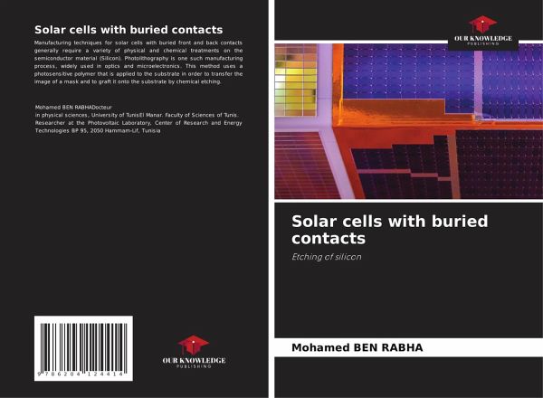
Solar cells with buried contacts
Etching of silicon
Versandkostenfrei!
Versandfertig in 6-10 Tagen
27,99 €
inkl. MwSt.

PAYBACK Punkte
14 °P sammeln!
Manufacturing techniques for solar cells with buried front and back contacts generally require a variety of physical and chemical treatments on the semiconductor material (Silicon). Photolithography is one such manufacturing process, widely used in optics and microelectronics. This method uses a photosensitive polymer that is applied to the substrate in order to transfer the image of a mask and to graft it onto the substrate by chemical etching.


