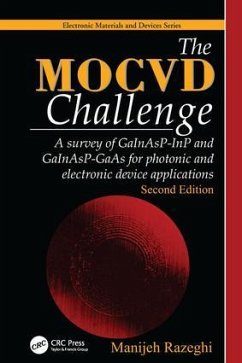
Written by one of the driving forces in the field, The MOCVD Challenge is a comprehensive review covering GaInAsP-InP, GaInAsP-GaAs, and related material for electronic and photonic device applications. These III-V semiconductor compounds have been used to realize the electronic, optoelectronic, and quantum devices that have revolutionized telecommunications. The figure on the back cover gives the energy gap and lattice parameter for the entire compositional range of the binary, ternary, and quaternary combinations of these III-V elements. By understanding the material and learning to control the growth new devices become possible: the front cover shows the world's first InP/GaInAs superlattice that was fabricated by the author - this has gone on to be the basis of modern quantum devices like quantum cascade lasers and quantum dot infrared photodetectors.
Now in its second edition, this updated and combined volume contains the secrets of MOCVD growth, material optimization, and modern device technology. It begins with an introduction to semiconductor compounds and the MOCVD growth process. It then discusses in situ and ex situ characterization for MOCVD growth. Next, the book examines in detail the specifics of the growth of GaInP(As)-GaAs and GaInAs(P)-InP material systems. It examines MOCVD growth of various III-V heterojunctions and superlattices and discusses electronic and optoelectronic devices realized with this material. Spanning 30 years of research, the book is the definitive resource on MOCVD.
Now in its second edition, this updated and combined volume contains the secrets of MOCVD growth, material optimization, and modern device technology. It begins with an introduction to semiconductor compounds and the MOCVD growth process. It then discusses in situ and ex situ characterization for MOCVD growth. Next, the book examines in detail the specifics of the growth of GaInP(As)-GaAs and GaInAs(P)-InP material systems. It examines MOCVD growth of various III-V heterojunctions and superlattices and discusses electronic and optoelectronic devices realized with this material. Spanning 30 years of research, the book is the definitive resource on MOCVD.
... a comprehensive review of GaInAsP-InP and GaInAsP-GaAs materials, III-V semiconductor compounds used for photonic and electronic device applications. This second edition represents the combined updated versions of the MOCVD Challenge. The author addresses a variety of relevant topics, including: growth technology, in situ characterization during MOCVD, ex situ characterization techniques, growth of GaAs layers, growth and characterization of the GaInP-GaAs system, optical devices, GaAs-based layers, optoelectronic integrated circuits, and optoelectronic devices on quantum structures.
-SciTech Book News, February 2011
-SciTech Book News, February 2011

