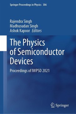
The Physics of Semiconductor Devices
Proceedings of IWPSD 2021
Herausgegeben:Singh, Rajendra; Singh, Madhusudan; Kapoor, Ashok
The Physics of Semiconductor Devices
Proceedings of IWPSD 2021
Herausgegeben:Singh, Rajendra; Singh, Madhusudan; Kapoor, Ashok
- Gebundenes Buch
- Merkliste
- Auf die Merkliste
- Bewerten Bewerten
- Teilen
- Produkt teilen
- Produkterinnerung
- Produkterinnerung
This book includes proceedings of the 21st International Workshop on Physics of Semiconductor Devices. The workshop is jointly organized by the Indian Institute of Technology, Delhi, and Solid State Physics Laboratory, Delhi, in collaboration with the Society for Semiconductor Devices and Semiconductor Society of India. This book disseminates the current knowledge of semiconductor physics and its applications across the scientific community. It is based on a biennial workshop that provides the participating research groups with a stimulating platform for interaction and collaboration with…mehr
Andere Kunden interessierten sich auch für
![The Physics of Semiconductor Devices The Physics of Semiconductor Devices]() The Physics of Semiconductor Devices227,99 €
The Physics of Semiconductor Devices227,99 €![The Physics of Semiconductors The Physics of Semiconductors]() Marius GrundmannThe Physics of Semiconductors40,99 €
Marius GrundmannThe Physics of Semiconductors40,99 €![The Physics of Semiconductors The Physics of Semiconductors]() Marius GrundmannThe Physics of Semiconductors123,04 €
Marius GrundmannThe Physics of Semiconductors123,04 €![Semiconductor Physics Semiconductor Physics]() Karl W. BöerSemiconductor Physics725,99 €
Karl W. BöerSemiconductor Physics725,99 €![Organic Photocurrent Multiplication Organic Photocurrent Multiplication]() Masahiro HiramotoOrganic Photocurrent Multiplication116,99 €
Masahiro HiramotoOrganic Photocurrent Multiplication116,99 €![The (Non-)Local Density of States of Electronic Excitations in Organic Semiconductors The (Non-)Local Density of States of Electronic Excitations in Organic Semiconductors]() Carl. R PoelkingThe (Non-)Local Density of States of Electronic Excitations in Organic Semiconductors77,99 €
Carl. R PoelkingThe (Non-)Local Density of States of Electronic Excitations in Organic Semiconductors77,99 €![The (Non-)Local Density of States of Electronic Excitations in Organic Semiconductors The (Non-)Local Density of States of Electronic Excitations in Organic Semiconductors]() Carl. R PoelkingThe (Non-)Local Density of States of Electronic Excitations in Organic Semiconductors77,99 €
Carl. R PoelkingThe (Non-)Local Density of States of Electronic Excitations in Organic Semiconductors77,99 €-
-
-
This book includes proceedings of the 21st International Workshop on Physics of Semiconductor Devices. The workshop is jointly organized by the Indian Institute of Technology, Delhi, and Solid State Physics Laboratory, Delhi, in collaboration with the Society for Semiconductor Devices and Semiconductor Society of India. This book disseminates the current knowledge of semiconductor physics and its applications across the scientific community. It is based on a biennial workshop that provides the participating research groups with a stimulating platform for interaction and collaboration with colleagues from the same scientific community. The book discusses the latest developments in III-nitrides; materials and devices, compound semiconductors, VLSI technology, optoelectronics, sensors, photovoltaics, crystal growth, epitaxy, and characterization, graphene, and other 2D materials and organic semiconductors. The research articles included in this book are contributed by various eminent scientists from all over the world. The book serves as a reference resource for researchers and practitioners in academia and industry.
Produktdetails
- Produktdetails
- Springer Proceedings in Physics 306
- Verlag: Springer / Springer Nature Singapore / Springer, Berlin
- Artikelnr. des Verlages: 978-981-97-1570-1
- 2024
- Seitenzahl: 432
- Erscheinungstermin: Mai 2024
- Englisch
- Abmessung: 241mm x 160mm x 28mm
- Gewicht: 832g
- ISBN-13: 9789819715701
- ISBN-10: 9819715709
- Artikelnr.: 69911947
- Herstellerkennzeichnung Die Herstellerinformationen sind derzeit nicht verfügbar.
Rajendra Singh is Professor at the Department of Physics, IIT Delhi, New Delhi since 2006. He received a Ph.D. degree from the Inter-University Accelerator Centre (affiliated to J.N.U., New Delhi) in 2001. He worked as Post-doctoral Fellow first at the Walter Schottky Institute, Technical University of Munich, Germany, and then at the Max Planck Institute of Microstructure Physics, Halle, Germany (2001-2006). His areas of interest are GaN-based materials and devices, wafer bonding, layer transfer of crystalline semiconductors and 2D materials, 2D materials and devices, 2D/3D heterojunctions. He has about 150 publications in International Journals and a similar number of publications in conference proceedings. Madhusudan Singh received his Ph.D. degree in Electrical Engineering from the University of Michigan, Ann Arbor, in 2005. After the post-doctoral experience at MIT, and research scientist experience at Arizona State, and serving as an Associate Editor for John Wiley,he joined the faculty of Department of Electrical Engineering, IIT Delhi in 2013 as Associate Professor. His research interests include solution-processed devices, flexible and printed electronics, materials chemistry, sensors and detectors, and general device physics. Ashok Kumar Kapoor received his Ph. D degree from the Department of Physics, Delhi University. He Joined Solid State Physics Laboratory, Delhi, in 1985 and superannuated as scientist 'G' and Group Head of Material Characterization group. His areas of research interest are the growth and characterization of semiconductor materials and conduction mechanisms in conducting polymers for solar cells and display applications for MBE growth of 2D metal chalcogenides. He has co-authored 35 publications in International and National journals and about 30 papers presented in various conferences and seminars. He has given several invited talks in various seminars and educational institutions.
Impact of Various Device Parameters on the Series Resistance of Perovskite Solar Cell.- Performance Investigation of Alkali Metal Fluorides as Alternate Electron Selective Contacts for TOPCon Solar Cells.- Computational Analysis of Antireflection Coatings for Semiconductor Solar Cells.- Effect of O2 Partial Pressure on Valence Band Maxima of HfO2 Thin Film.- Dependence of analog performance and linearity with channel doping concentration for an InGaAs MOSFET.- Effect of Channel Epilayer Thickness on Low Power Analog Operation of Asymmetric U-Shaped pTFET.- Effect of Helium gas addition to SF6/O2 chemistry for SiC dry etching in AlGaN/GaN/SiC HEMTs.- Modeling of High and Low Resistant States inSingle Defect Atomristors.- Design of Vertical Superjunction AlGaN/GaN HEMT: A TCAD-based Approach.- Effect on photo-absorbance and optical energy-gap of Al2O3 thin film after deposition of Ag thin film.- Thermometry across switching oxide layer in ReRAM device.- Effective Mobility Extraction of GaN-HEMTusing S-parameter.- Stress Dependent Electrical Characteristics of Flexible a-IGZO TFTs.- Modeling of Negative Capacitance Field effect transistors based on different ferroelectric materials.- Comparative Investigation of Single and Double Channel AlGaN/GaN HEMTs for LNAs.- ZnO nanorods orientation control with seedless hydrothermal growth and finding suitable morphology with simulation for tactile sensors.- A Comparative Demonstration of a 2D MXene-based Asymmetric Memristor Using Pristine and Nanohybrid Ti3C2Tx.- Modelling and simulation of a thin-film bulk acoustic resonator (FBAR) based gas sensor.- Design and Simulation of an open EWOD based Digital Microfluidic Device for Droplet Actuation using COMSOL.- A Capacitive Transducer for film Thickness Measurement.- Performance Projection of Stacked Silicon Nanosheet-FET Architectures for Future Technology Node.- Determination of Coupling Coefficient in Large Optical Cavity Distributed Feedback Laser structure with metal surfacegrating.- Design and Simulation of Stepped Microcantilevers for Energy Harvesting Applications.- Lowering Motional Impedance in Micromachined Frequency-Synthesizer Using Ultra-thin (SiO2 ~30 nm) Internal Dielectric.- Thermally Synthesized Cu/CuO/Cu(sheet) with Bipolar Resistive Switching.- Dynamic tuning of ENZ region of ITO and sensing using a tapered optical fiber.- Identifying the Recombination Zone in Perovskite Solar Cells.- High speed etching of silicon in NaOH-based solution using Surface to Volume Ratio (SVR).- Parylene membrane transfer on PDMS microchannel for microvalve fabrication.- RF Analysis of Tapered Angle Hetero-junction Dopingless TFET for low power applications.- Impact of pocket doped Mg2Si/Si hetrojunction Ge gated TFET for low optical power detection at 1550 nm.- MEMS acoustic sensor for low frequency applications.- Aptamer functionalized CVD grown monolayer WS2 based FETs for real-time detection of E. coli.- Superconducting stub tuner impedance matching circuitfor high-frequency measurements of nanoscale devices.- Spice Simulation of Solution Processed Bottom Gate Bottom Contact Organic Thin Film Transistor.- Inducing Phase transitions in MoS2 by Ionic liquid gating.- Ultrasensitive reduced vanadium dioxidebased MEMS Pirani gauge with extended dynamic range.- Lower Drying Temperature Process for Hole Transport Layer PEDOT: PSS in PCDTBT: PCBM Devices.- Electrical Performance of Protein-based Flexible MIM Structure Fabricated at Room Temperature for Proteotronic Applications.- Estimation of asymmetrically distributed anti-phase domains ratio in GaAs/Si(100) epitaxial layers using high resolution X-ray diffraction.- A Vertical GaN Split Gate Trench MOSFET Device with Reduced Switching Energy Losses.- Optimization of Negative Differential Conductance (NDC) Point for Multi Gate Devices Considering Self Heating Effects using Surface to Volume Ratio (SVR).- Performance of Strained-SiGe in FinFETs and Stacked Nanosheet FETs for Sub-7nm TechnologyNode.- Thermal Admittance Spectroscopy of AlGaN/GaN HEMT Structure.- Numerical Modelling of WO3-based Memristive System for Neuromorphic Computation.- Flexible Organic Field-Effect Transistor using Natural Protein as a Gate Dielectric for Green Electronics.- Design and Analysis of Cs3Sb2Br9/Si Tandem Solar Cell using SCAPS-1D.- One-pot preparation of Fe/Cu catalytic solution for the growth of carbon nanotubes for use in gas sensor and field emission devices.
Impact of Various Device Parameters on the Series Resistance of Perovskite Solar Cell.- Performance Investigation of Alkali Metal Fluorides as Alternate Electron Selective Contacts for TOPCon Solar Cells.- Computational Analysis of Antireflection Coatings for Semiconductor Solar Cells.- Effect of O2 Partial Pressure on Valence Band Maxima of HfO2 Thin Film.- Dependence of analog performance and linearity with channel doping concentration for an InGaAs MOSFET.- Effect of Channel Epilayer Thickness on Low Power Analog Operation of Asymmetric U-Shaped pTFET.- Effect of Helium gas addition to SF6/O2 chemistry for SiC dry etching in AlGaN/GaN/SiC HEMTs.- Modeling of High and Low Resistant States inSingle Defect Atomristors.- Design of Vertical Superjunction AlGaN/GaN HEMT: A TCAD-based Approach.- Effect on photo-absorbance and optical energy-gap of Al2O3 thin film after deposition of Ag thin film.- Thermometry across switching oxide layer in ReRAM device.- Effective Mobility Extraction of GaN-HEMTusing S-parameter.- Stress Dependent Electrical Characteristics of Flexible a-IGZO TFTs.- Modeling of Negative Capacitance Field effect transistors based on different ferroelectric materials.- Comparative Investigation of Single and Double Channel AlGaN/GaN HEMTs for LNAs.- ZnO nanorods orientation control with seedless hydrothermal growth and finding suitable morphology with simulation for tactile sensors.- A Comparative Demonstration of a 2D MXene-based Asymmetric Memristor Using Pristine and Nanohybrid Ti3C2Tx.- Modelling and simulation of a thin-film bulk acoustic resonator (FBAR) based gas sensor.- Design and Simulation of an open EWOD based Digital Microfluidic Device for Droplet Actuation using COMSOL.- A Capacitive Transducer for film Thickness Measurement.- Performance Projection of Stacked Silicon Nanosheet-FET Architectures for Future Technology Node.- Determination of Coupling Coefficient in Large Optical Cavity Distributed Feedback Laser structure with metal surfacegrating.- Design and Simulation of Stepped Microcantilevers for Energy Harvesting Applications.- Lowering Motional Impedance in Micromachined Frequency-Synthesizer Using Ultra-thin (SiO2 ~30 nm) Internal Dielectric.- Thermally Synthesized Cu/CuO/Cu(sheet) with Bipolar Resistive Switching.- Dynamic tuning of ENZ region of ITO and sensing using a tapered optical fiber.- Identifying the Recombination Zone in Perovskite Solar Cells.- High speed etching of silicon in NaOH-based solution using Surface to Volume Ratio (SVR).- Parylene membrane transfer on PDMS microchannel for microvalve fabrication.- RF Analysis of Tapered Angle Hetero-junction Dopingless TFET for low power applications.- Impact of pocket doped Mg2Si/Si hetrojunction Ge gated TFET for low optical power detection at 1550 nm.- MEMS acoustic sensor for low frequency applications.- Aptamer functionalized CVD grown monolayer WS2 based FETs for real-time detection of E. coli.- Superconducting stub tuner impedance matching circuitfor high-frequency measurements of nanoscale devices.- Spice Simulation of Solution Processed Bottom Gate Bottom Contact Organic Thin Film Transistor.- Inducing Phase transitions in MoS2 by Ionic liquid gating.- Ultrasensitive reduced vanadium dioxidebased MEMS Pirani gauge with extended dynamic range.- Lower Drying Temperature Process for Hole Transport Layer PEDOT: PSS in PCDTBT: PCBM Devices.- Electrical Performance of Protein-based Flexible MIM Structure Fabricated at Room Temperature for Proteotronic Applications.- Estimation of asymmetrically distributed anti-phase domains ratio in GaAs/Si(100) epitaxial layers using high resolution X-ray diffraction.- A Vertical GaN Split Gate Trench MOSFET Device with Reduced Switching Energy Losses.- Optimization of Negative Differential Conductance (NDC) Point for Multi Gate Devices Considering Self Heating Effects using Surface to Volume Ratio (SVR).- Performance of Strained-SiGe in FinFETs and Stacked Nanosheet FETs for Sub-7nm TechnologyNode.- Thermal Admittance Spectroscopy of AlGaN/GaN HEMT Structure.- Numerical Modelling of WO3-based Memristive System for Neuromorphic Computation.- Flexible Organic Field-Effect Transistor using Natural Protein as a Gate Dielectric for Green Electronics.- Design and Analysis of Cs3Sb2Br9/Si Tandem Solar Cell using SCAPS-1D.- One-pot preparation of Fe/Cu catalytic solution for the growth of carbon nanotubes for use in gas sensor and field emission devices.

