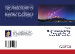
The Synthesis & Optical Characterization of Doped CdS Thin Films
Versandkostenfrei!
Versandfertig in 6-10 Tagen
27,99 €
inkl. MwSt.

PAYBACK Punkte
14 °P sammeln!
Among the wide band gap II-VI semiconductors, cadmium sulphide (CdS) with its direct band gap of 2.42 eV at room temperature is of great importance, because they are potentially promising materials and is applied in wide variety of fields such as solar cells, light emitting diodes, thin film FET transistors, and photonic devices. In general, un-doped CdS thin films are highly resistive and considerable decrease in resistivity could be achieved by a careful control of stoichiometry. As far as solarcell applications are concerned low resistivity and large grain sized materials are desirable, and...
Among the wide band gap II-VI semiconductors, cadmium sulphide (CdS) with its direct band gap of 2.42 eV at room temperature is of great importance, because they are potentially promising materials and is applied in wide variety of fields such as solar cells, light emitting diodes, thin film FET transistors, and photonic devices. In general, un-doped CdS thin films are highly resistive and considerable decrease in resistivity could be achieved by a careful control of stoichiometry. As far as solarcell applications are concerned low resistivity and large grain sized materials are desirable, and that can be achieved by incorporating some doping into CdS thin films. The optical properties of these films may be tuned by varying the composition and atomic ordering. The chemical bath deposition (CBD) is known to be a simple, low temperature, and inexpensive large-area deposition technique. Annealing is a traditional but very useful method to improve the crystalline and optical properties of semiconductor materials including crystal grain alignment, change in crystallite size and optical band gap.


