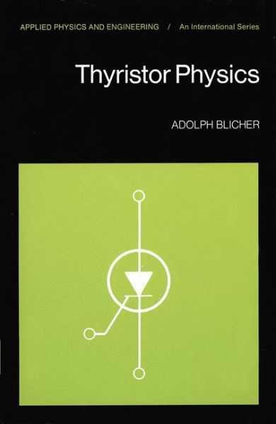
In this volume I attempt to present concisely the physical principles underlying the operation and performance characteristics of the class of semiconductor p-n-p-n switches known as thyristors. The semiconductor controlled rectifier (SCR), the triode AC switch (Triac) the gate turn-off switch (GTO), and the reverse conducting thyristor (RCT) are some of the most important devices belonging to this device family. This book is aimed both at semiconductor-device physicists, designers, and students and at those electronic circuit designers who wish to apply thyristors creatively without the…mehr
In this volume I attempt to present concisely the physical principles underlying the operation and performance characteristics of the class of semiconductor p-n-p-n switches known as thyristors. The semiconductor controlled rectifier (SCR), the triode AC switch (Triac) the gate turn-off switch (GTO), and the reverse conducting thyristor (RCT) are some of the most important devices belonging to this device family. This book is aimed both at semiconductor-device physicists, designers, and students and at those electronic circuit designers who wish to apply thyristors creatively without the limitation of con sidering them as "black boxes," described only by insufficiently understood electrical ratings. The book endeavors to present an up-to-date account of the progress made in understanding the operation, potentialities, and limitations of thyristors as switching circuit elements. It assumes some basic knowledge of transistor physics and stresses the phe nomenological aspects of thyristor theory with the use of mathe matics not going beyond calculus and differential equations. The first two chapters discuss basic thyristor operation theory. The sub sequent chapters are devoted to the study of the static and dynamic properties of the SCR, the RCT, the GTO, and the triac; they in clude discussions of forward voltage drops, maximum voltage blocking capabilities, turn-on and turn-off transients, current and voltage rise rates, and desirable and undesirable triggering effects.Hinweis: Dieser Artikel kann nur an eine deutsche Lieferadresse ausgeliefert werden.
1 Device basics.- 1.1 Introduction.- 1.2 SCR current-voltage characteristics.- 1.3 Basic SCR construction features.- 1.4 Gate triggering.- 1.5 Holding current.- 1.6 Triggering a shorted emitter SCR.- 2 Current Gain.- 2.1 Variation of current gain with current.- 2.2 Current gain measurement.- 3 Thyristor Maximum Voltage Blocking Capability.- 3.1 Introduction.- 3.2 Maximum forward-blocking capability VBO.- 3.3 Maximum reverse-blocking capability.- 3.4 The punch-through condition.- 3.5 Temperature dependence.- 3.6 Surface breakdown.- 3.7 Reverse-conducting thyristor.- 4 Some High-Injection-Level Effects.- 4.1 Introduction.- 4.2 Ambipolar mobility and diffusivity.- 4.3 Mobility and diffusivity versus current density.- 4.4 Lifetime at high injection levels.- 4.5 High-low junctions at high current densities.- 4.6 Current gain fall-off.- 5 The Gate-Triggered SCR Turn-On Transient.- 5.1 Introduction.- 5.2 Charge-control model of a bipolar transistor.- 5.3 Charge-control model of a p-n-p-n structure.- 5.4 Delay time.- 5.5 Rise time with a resistive load.- 5.6 Rise time with inductive load.- 5.7 Propagation of the on state.- 6 The Nongated, Undesirable Thyristor Triggering.- 6.1 Introduction.- 6.2 Thermal turn on.- 6.3 Light triggering.- 6.4 Voltage triggering.- 7 Thyristor Voltage Drop in the On State.- 7.1 Introduction.- 7.2 Herlet's closed-form p-i-n diode analysis.- 7.3 Kokosa's numerical analysis.- 7.4 Numerical analysis of Cornu and Lietz.- 7.5 Otsuka's forward-drop analysis.- 8 SCR Turn-off Transient.- 8.1 Introduction.- 8.2 Storage time ts1.- 8.3 Fall time tf1.- 8.4 Storage time ts2.- 8.5 Fall time tf2.- 8.6 Effect of the gate current.- 8.7 Simplified approaches.- 8.8 Experimental data.- 9 Gate Turn-off Thyristor (GTO).- 9.1 Introduction.- 9.2 Plasma-pinchingmechanism.- 9.3 Turn-off velocity.- 9.4 Pinching (focusing) time and turn-off gain.- 9.5 Maximum anode and gate currents.- 9.6 Plasma-pinching in the ungated n base.- 9.7 Theoretical model compared with experiment.- 10 Thyristor di/dt and Current Pulse Capability.- 10.1 Introduction.- 10.2 Test circuit for gate-triggered di/dt.- 10.3 Initial turn-on region.- 10.4 di/dt capability of the gated and nongated turn on.- 10.5 Localized temperature rise for a short single pulse.- 10.5 Temperature rise for long or recurrent pulses.- 10.7 Temperature rise and transient thermal impedance during turn-on spreading.- 10.8 Methods of increasing the initial turn-on area.- 10.9 Emitter gate.- 10.10 Emitter shorts versus the turn-on time.- 10.11 Beam-fired thyristor.- 10.12 Field-controlled thyristor.- 11 Bidirectional p-n-p-n Switches.- 11.1 Introduction.- 11.2 Bidirectional p-n-p-n diode switch.- 11.3 Current distribution across a forward-biased junction bounded by resistive layers (current-crowding effect).- 11.4 Junction gate.- 11.5 Remote gate.- 11.6 Triac.- 12 Commutation of Triacs.- 12.1 Introduction.- 12.2 Current and voltage waveforms during commutation.- 12.3 Role of stored charges in triac commutation.- 12 A Recovery of a p+ -n abrupt-junction diode.- 12.5 Snubber networks for dv/dt suppression.- 13 Silicon Surface.- 13.1 Introduction.- 13.2 Ideal MOS diode.- 13.3 Silicon surf ace states and charges.- 14 Avalanche Breakdown Enhancement by Mesa Contouring.- 14.1 Introduction.- 14.2 Positive and negative bevel angles.- 14.3 Theoretical approach to the field computation in the depletion region.- 14.4 Negative bevel angle.- 14.5 Positively beveled junctions.- 14.6 Novel approaches to beveling.- 15 Planar-Junction Avalanche Breakdown Improvement.- 15.1 Introduction.- 15.2 Diffused guard ring.- 15.3 Junction field plate, annular ring, and channel stopper.- 15.4 Resistive field plate.- 15.5 p-n junction with field limiting rings.- 15.6 Etch-contoured planar junctions.- 16 Thyristor Thermal Response.- 16.1 Introduction.- 16.2 Heat generation and absorption in the forward-biased thyristor.- 16.3 Determination of junction temperature.- 16.4 Generalized concept of thermal impedance.- 16.5 Device temperature response to an arbitrary power waveshape.- 16.6 Thyristor thermal impedance measurement.- 16.7 Computer-aided thermal analysis.- 17 Thyristor Circuits Basics.- 17.1 Introduction.- 17.2 SCR and triac control and triggering methods.- 17.3 Thyristor triggering devices.- 17.4 Commutation.- 17.5 Effect of an impedance between the gate and cathode of a thyristor.- 17.6 Thyristor protection circuits.- 17.7 Some thyristor applications.
Es gelten unsere Allgemeinen Geschäftsbedingungen: www.buecher.de/agb
Impressum
www.buecher.de ist ein Internetauftritt der Steintor 70. V V GmbH (zukünftig firmierend: buecher.de internetstores GmbH)
Geschäftsführung: Monica Sawhney | Roland Kölbl
Sitz der Gesellschaft: Hannover
Amtsgericht Hannover HRB 227001
Steuernummer: 321/neu