Alain Claverie
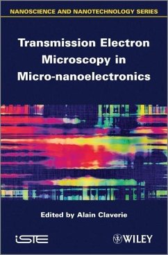
Transmission Electron Microscopy in Micro-Nanoelectronics
Alain Claverie
Transmission Electron Microscopy in Micro-Nanoelectronics
- Gebundenes Buch
- Merkliste
- Auf die Merkliste
- Bewerten Bewerten
- Teilen
- Produkt teilen
- Produkterinnerung
- Produkterinnerung
Today, the availability of bright and highly coherent electron sources and sensitive detectors has radically changed the type and quality of the information which can be obtained by transmission electron microscopy (TEM). TEMs are now present in large numbers not only in academia, but also in industrial research centers and fabs. This book presents in a simple and practical way the new quantitative techniques based on TEM which have recently been invented or developed to address most of the main challenging issues scientists and process engineers have to face to develop or optimize…mehr
Andere Kunden interessierten sich auch für
![Semiconductor Device and Failure Analysis Semiconductor Device and Failure Analysis]() Wai Kin ChimSemiconductor Device and Failure Analysis275,99 €
Wai Kin ChimSemiconductor Device and Failure Analysis275,99 €![Nanoscale Microwave Engineerin Nanoscale Microwave Engineerin]() Charlotte Tripon-CanselietNanoscale Microwave Engineerin194,99 €
Charlotte Tripon-CanselietNanoscale Microwave Engineerin194,99 €![Micro and Smart Systems Micro and Smart Systems]() G K AnanthasureshMicro and Smart Systems229,99 €
G K AnanthasureshMicro and Smart Systems229,99 €![Nano Lithography Nano Lithography]() Nano Lithography191,99 €
Nano Lithography191,99 €![Scanning Transmission Electron Microscopy Scanning Transmission Electron Microscopy]() Scanning Transmission Electron Microscopy178,99 €
Scanning Transmission Electron Microscopy178,99 €![Audiovisual Archives Audiovisual Archives]() Audiovisual Archives216,99 €
Audiovisual Archives216,99 €![Wireless Optical Communications Wireless Optical Communications]() Olivier BouchetWireless Optical Communications197,99 €
Olivier BouchetWireless Optical Communications197,99 €-
-
-
Today, the availability of bright and highly coherent electron sources and sensitive detectors has radically changed the type and quality of the information which can be obtained by transmission electron microscopy (TEM). TEMs are now present in large numbers not only in academia, but also in industrial research centers and fabs.
This book presents in a simple and practical way the new quantitative techniques based on TEM which have recently been invented or developed to address most of the main challenging issues scientists and process engineers have to face to develop or optimize semiconductor layers and devices. Several of these techniques are based on electron holography; others take advantage of the possibility of focusing intense beams within nanoprobes. Strain measurements and mappings, dopant activation and segregation, interfacial reactions at the nanoscale, defect identification and specimen preparation by FIB are among the topics presented in this book. After a brief presentation of the underlying theory, each technique is illustrated through examples from the lab or fab.
Hinweis: Dieser Artikel kann nur an eine deutsche Lieferadresse ausgeliefert werden.
Produktdetails
- Produktdetails
- ISTE .
- Verlag: Wiley & Sons
- 1. Auflage
- Seitenzahl: 264
- Erscheinungstermin: 26. Dezember 2012
- Englisch
- Abmessung: 236mm x 155mm x 20mm
- Gewicht: 590g
- ISBN-13: 9781848213678
- ISBN-10: 1848213670
- Artikelnr.: 36063333
- Herstellerkennzeichnung
- Libri GmbH
- Europaallee 1
- 36244 Bad Hersfeld
- gpsr@libri.de
Alain Claverie is Directeur of CEMES/CNRS, Toulouse, France.
Introduction xi
Chapter 1. Active Dopant Profiling in the TEM by Off-Axis Electron
Holography 1
David COOPER
1.1. Introduction 1
1.2. The Basics: from electron waves to phase images 3
1.2.1. Electron holography for the measurement of electromagnetic fields
3
1.2.2. The electron source 6
1.2.3. Forming electron holograms using an electron biprism 6
1.2.4. Care of the electron biprism 10
1.2.5. Recording electron holograms 11
1.2.6. Hologram reconstruction 12
1.2.7. Phase Jumps 15
1.3. Experimental electron holography 16
1.3.1. Fringe contrast, sampling and phase sensitivity 16
1.3.2. Optimizing the beam settings for an electron holography
experiment 20
1.3.3. Optimizing the field of view using free lens control 21
1.3.4. Energy filtering for electron holography 24
1.3.5. Minimizing diffraction contrast 25
1.3.6. Measurement of the specimen thickness 26
1.3.7. Specimen preparation 28
1.3.8. The electrically inactive thickness 30
1.4. Conclusion 33
1.5. Bibliography 33
Chapter 2. Dopant Distribution Quantitative Analysis Using STEM-EELS/EDX
Spectroscopy Techniques 37
Roland PANTEL and Germain SERVANTON
2.1. Introduction 37
2.1.1. Dopant analysis challenges in the silicon industry 37
2.1.2. The different dopant quantification and imaging methods 38
2.2. STEM-EELS-EDX experimental challenges for quantitative dopant
distribution analysis 41
2.2.1. Instrumentation present state-of-the-art and future challenges 41
2.3. Experimental conditions for STEM spectroscopy impurity detection 43
2.3.1. Radiation damages 43
2.3.2. Particularities of EELS and EDX spectroscopy techniques 44
2.3.3. Equipments used for the STEM-EELS-EDX analyses presented in this
chapter 49
2.4. STEM EELS-EDX quantification of dopant distribution application
examples 49
2.4.1. EELS application analysis examples 49
2.4.2. EDX application analysis examples 54
2.5. Discussion on the characteristics of STEM-EELS/EDX and data
processing 59
2.6. Bibliography 59
Chapter 3. Quantitative Strain Measurement in Advanced Devices: A
Comparison Between Convergent Beam Electron Diffraction and Nanobeam
Diffraction 65
Laurent CLÉMENT and Dominique DELILLE
3.1. Introduction 65
3.2 Electron diffraction technique in TEM (CBED and NBD) 66
3.2.1. CBED patterns acquisition and analysis 66
3.2.2. NBD patterns acquisition and analysis 70
3.3. Experimental details 71
3.3.1. Instrumentation and setup 71
3.3.2. Samples description 72
3.4. Results and discussion 72
3.4.1. Strain evaluation in a pMOS transistor integrating eSiGe source and
drain - a comparison of CBED and NBD techniques 72
3.4.2. Quantitative strain measurement in advanced devices by NBD 75
3.5. Conclusion 78
3.6. Bibliography 78
Chapter 4. Dark-Field Electron Holography for Strain Mapping 81
Martin HTCH, Florent HOUDELLIER, Nikolay CHERKASHIN, Shay REBO, Elsa
JAVON, P t c BENZO, Christophe GATEL, Etienne SNOECK and Alain CLAVERIE
4.1. Introduction 81
4.2. Setup for dark-field electron holography 83
4.3. Experimental requirements 85
4.4. Strained silicon transistors with recessed sources and drains
stressors 87
4.4.1. Strained silicon p-MOSFET 87
4.5. Thin film effect 92
4.6. Silicon implanted with hydrogen 93
4.7. Strained silicon n-MOSFET 94
4.8. Understanding strain engineering 96
4.9. Strained silicon devices relying on stressor layers 97
4.10. 28-nm technology node MOSFETs 99
4.11. FinFET device 101
4.12. Conclusions 103
4.13. Bibliography 103
Chapter 5. Magnetic Mapping Using Electron Holography 107
Etienne SNOECK and Christophe GATEL
5.1. Introduction 107
5.2. Experimental 108
5.2.1. The Lorentz mode 110
5.2.2 The "¿E" problem 111
5.3. Hologram analysis: from the phase images to the magnetic properties
118
5.3.1. The simplest case: homogeneous specimen of constant thickness 119
5.3.2. The general case 122
5.4. Resolutions 124
5.4.1. Magnetic measurements accuracy 124
5.4.2. Spatial resolution 126
5.5. One example: FePd (L10) epitaxial thin film exhibiting a perpendicular
magnetic anisotropy (PMA) 126
5.6. Prospective and new developments 130
5.6.1. Enhanced signal and resolution 130
5.6.2. In-situ switching 131
5.7. Conclusions 132
5.8. Bibliography 133
Chapter 6. Interdiffusion and Chemical Reaction at Interfaces by TEM/EELS
135
Sylvie SCHAMM-CHARDON
6.1. Introduction 135
6.2. Importance of interfaces in MOSFETs 135
6.3. TEM and EELS 137
6.4. TEM/EELS and study of interdiffusion/chemical reaction at interfaces
in microelectronics 137
6.4.1. Thickness measurement 138
6.4.2. Atomic structure analysis 139
6.4.3. EELS analysis 141
6.4.4. Sample preparation 143
6.5. HRTEM/EELS as a support to developments of RE- and TM-based HK thin
films on Si and Ge 144
6.5.1. Introduction 144
6.5.2. HRTEM/EELS methodology 145
6.5.3. Illustrations 154
6.6. Conclusion 158
6.7 Bibliography 158
Chapter 7. Characterization of Process-Induced Defects 165
Nikolay CHERKASHIN and Alain CLAVERIE.
7.1. Interfacial dislocations 166
7.1.1. Si(100)/Si(100) direct wafer bonding (DWB) 167
7.1.2. SiGe heterostructures 170
7.2. Ion implantation induced defects 172
7.2.1. Defects of interstitial type 173
7.2.2. Defects of vacancy type 187
7.3. Conclusions 193
7.4. Bibliography 193
Chapter 8. In Situ Characterization Methods in Transmission Electron
Microscopy 199
Aurélien MASSEBOEUF
8.1. Introduction 199
8.2. In situ in a TEM 200
8.2.1. Temperature control and irradiation 201
8.2.2. Electromagnetic field 201
8.2.3. Mechanical 202
8.2.4. Chemistry 202
8.2.5. Light 203
8.2.6. Multiple and movable currents 203
8.3. Biasing in a conventional TEM 204
8.3.1. Multiple contacts 204
8.3.2. Movable contacts 206
8.3.3. Comparison 206
8.4. Sample design 208
8.4.1. Focused ion beam 208
8.4.2. TEM windows 209
8.5. Conclusions 211
8.6. Biblioraphy 211
Chapter 9. Specimen Preparation for Semiconductor Analysis 219
David COOPER and Gérard BEN ASSAYAG
9.1. The focused ion beam tool 220
9.2. Ion-sample interaction 221
9.3. Beam currents and energies for specimen preparation 225
9.4. Practical specimen preparation 228
9.5. In situ lift-out 228
9.6. H-bar technique 232
9.7. Broad beam ion milling 233
9.8. Mechanical wedge polishing 235
9.9. Conclusion 235
9.10 Bibliography 236
List of Authors 237
Index 241

