HattoriSecrets of VLSI Manufacturing
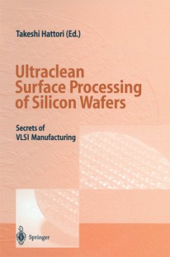
Ultraclean Surface Processing of Silicon Wafers
Secrets of VLSI Manufacturing
Herausgegeben:Hattori, Takeshi;Übersetzung:Hattori, T.; Heusler, S.; Webb, J.P.
HattoriSecrets of VLSI Manufacturing
Ultraclean Surface Processing of Silicon Wafers
Secrets of VLSI Manufacturing
Herausgegeben:Hattori, Takeshi;Übersetzung:Hattori, T.; Heusler, S.; Webb, J.P.
- Gebundenes Buch
- Merkliste
- Auf die Merkliste
- Bewerten Bewerten
- Teilen
- Produkt teilen
- Produkterinnerung
- Produkterinnerung
A totally new concept for clean surface processing of Si wafers is introduced in this book. Some fifty distinguished researchers and engineers from the leading Japanese semiconductor companies, such as NEC, Hitachi, Toshiba, Sony and Panasonic as well as from several universities reveal to us for the first time the secrets of these highly productive institutions. They describe the techniques and equipment necessary for the preparation of clean high-quality semiconductor surfaces as a first step in high-yield/high-quality device production. This book thus opens the door to the manufacturing of…mehr
Andere Kunden interessierten sich auch für
![Shape and Functional Elements of the Bulk Silicon Microtechnique Shape and Functional Elements of the Bulk Silicon Microtechnique]() Joachim FrühaufShape and Functional Elements of the Bulk Silicon Microtechnique91,99 €
Joachim FrühaufShape and Functional Elements of the Bulk Silicon Microtechnique91,99 €![Integrated Silicon Optoelectronics Integrated Silicon Optoelectronics]() Horst ZimmermannIntegrated Silicon Optoelectronics112,99 €
Horst ZimmermannIntegrated Silicon Optoelectronics112,99 €![Silicone Composite Insulators Silicone Composite Insulators]() Konstantin O. PapailiouSilicone Composite Insulators112,99 €
Konstantin O. PapailiouSilicone Composite Insulators112,99 €![Physics and Technology of Amorphous-Crystalline Heterostructure Silicon Solar Cells Physics and Technology of Amorphous-Crystalline Heterostructure Silicon Solar Cells]() Physics and Technology of Amorphous-Crystalline Heterostructure Silicon Solar Cells163,99 €
Physics and Technology of Amorphous-Crystalline Heterostructure Silicon Solar Cells163,99 €![Silicon Photonics Silicon Photonics]() Lorenzo Pavesi / David J. Lockwood (eds.)Silicon Photonics242,99 €
Lorenzo Pavesi / David J. Lockwood (eds.)Silicon Photonics242,99 €![Integrated Silicon Optoelectronics Integrated Silicon Optoelectronics]() Horst ZimmermannIntegrated Silicon Optoelectronics121,99 €
Horst ZimmermannIntegrated Silicon Optoelectronics121,99 €![Silicone Composite Insulators Silicone Composite Insulators]() Konstantin O. PapailiouSilicone Composite Insulators112,99 €
Konstantin O. PapailiouSilicone Composite Insulators112,99 €-
-
-
A totally new concept for clean surface processing of Si wafers is introduced in this book. Some fifty distinguished researchers and engineers from the leading Japanese semiconductor companies, such as NEC, Hitachi, Toshiba, Sony and Panasonic as well as from several universities reveal to us for the first time the secrets of these highly productive institutions. They describe the techniques and equipment necessary for the preparation of clean high-quality semiconductor surfaces as a first step in high-yield/high-quality device production. This book thus opens the door to the manufacturing of reliable nanoscale devices and will be extremely useful for every engineer, physicist and technician involved inthe production of silicon semiconductor devices.
Produktdetails
- Produktdetails
- Verlag: Springer / Springer Berlin Heidelberg / Springer, Berlin
- Artikelnr. des Verlages: 978-3-540-61672-6
- 1998.
- Seitenzahl: 616
- Englisch
- Abmessung: 238mm x 153mm x 44mm
- Gewicht: 890g
- ISBN-13: 9783540616726
- ISBN-10: 3540616721
- Artikelnr.: 07509554
- Herstellerkennzeichnung Die Herstellerinformationen sind derzeit nicht verfügbar.
Takeshi Hattori does research and development of cellular systems, paging systems, maritime systems, and advanced cordless systems at NTT.
I. Introduction.- 1. Ultraclean Technology for VLSI Manufacturing: An Overview.- II. Influence of Contamination on Silicon Device Characteristics.- 2. Influence of Silicon Crystal Quality on Device Characteristics.- 3. Influence of Contaminants on Device Characteristics.- 4. Influence of Metallic Contamination on Dielectric Degradation of MOS Structures.- 5. Influence of Micro-Roughness on Device Characteristics.- III. Mechanisms of Particle Adhesion on Wafer Surfaces.- 6. Particle Deposition in Air.- 7. Particle Deposition in Plasma.- 8. Particle Deposition in Vacuum.- 9. Particle Adhesion in Liquids.- 10. Particle Adhesion and Removal on Wafer Surfaces in RCA Cleaning.- 11. Effects of Electrostatic Charge on Particle Adhesion on Wafer Surfaces.- IV. Analysis and Evaluation of Silicon Wafer Surfaces: Fundamentals.- 12. Measurement of Particles on Wafer Surfaces.- 13. Analysis and Evaluation of Impurities on Wafer Surfaces.- 14. Analysis and Evaluation of Molecules Adhered to Wafer Surfaces.- 15. Electrical Evaluation of Metallic Impurities on Wafer Surfaces.- 16. Analysis of Microscopic Areas on Wafer Surfaces Using STM/AFM.- V. Analysis and Evaluation of Wafer Surfaces: Applications to Semiconductor Manufacturing Lines.- 17. Detection and Analysis of Particles in Production Lines.- 18. Pattern Defect Monitoring in Production Lines.- 19. Clean Level Monitoring in Production Lines.- 20. Analysis of Defects in Devices and Silicon Crystals in Production Lines.- VI. Ultraclean Technology for Wafer Processes and Equipment.- 21. Oxidation and Diffusion.- 22. CVD (Part 1): Atmospheric Pressure/Low-Pressure CVD.- 23. CVD (Part 2): Plasma CVD.- 24. CVD (Part 3): Metal CVD.- 25. Physical Vapor Deposition.- 26. Dry Etching (Part 1): Particulate Contamination Due to Dry Etching.-27. Dry Etching (Part 2): Influence of Chemical Contamination and Defects on Dry Etching.- 28. Ion Implantation.- 29. Lithography.- 30. CMP.- 31. Cluster Tools.- VII. Cleaning Silicon Wafer Surfaces.- 32. Trends in Wafer Cleaning Technology.- 33. Wet Cleaning (Part 1): Removal of Particulate Contaminants.- 34. Wet Cleaning (Part 2): Removal of Metallic Contaminants.- 35. Wet Cleaning (Part 3): Removal of Organic Contaminants.- 36. Wet Cleaning (Part 4): Micro-Roughness and COPs Created by SC-1.- 37. Wafer Drying After Wet Cleaning.- 38. Watermarks: Generation, Control, and Removal.- 39. Physical Cleaning.- 40. Dry Cleaning.- VIII. Wafer-Cleaning-Related Issues.- 41. HF Vapor Cleaning Technology.- 42. Native Oxide Films and Chemical Oxide Films.- 43. Hydrogen Termination: The Ideally Finished Silicon Surface.- 44. Adsorption of Organic Volatiles on Silicon Surfaces and Their Removal by Wet Cleaning.- 45. Wafer Carrier Cleaning.- 46. Goals for Next-Generation Wafer Cleaning Technology.
I. Introduction.- 1. Ultraclean Technology for VLSI Manufacturing: An Overview.- II. Influence of Contamination on Silicon Device Characteristics.- 2. Influence of Silicon Crystal Quality on Device Characteristics.- 3. Influence of Contaminants on Device Characteristics.- 4. Influence of Metallic Contamination on Dielectric Degradation of MOS Structures.- 5. Influence of Micro-Roughness on Device Characteristics.- III. Mechanisms of Particle Adhesion on Wafer Surfaces.- 6. Particle Deposition in Air.- 7. Particle Deposition in Plasma.- 8. Particle Deposition in Vacuum.- 9. Particle Adhesion in Liquids.- 10. Particle Adhesion and Removal on Wafer Surfaces in RCA Cleaning.- 11. Effects of Electrostatic Charge on Particle Adhesion on Wafer Surfaces.- IV. Analysis and Evaluation of Silicon Wafer Surfaces: Fundamentals.- 12. Measurement of Particles on Wafer Surfaces.- 13. Analysis and Evaluation of Impurities on Wafer Surfaces.- 14. Analysis and Evaluation of Molecules Adhered to Wafer Surfaces.- 15. Electrical Evaluation of Metallic Impurities on Wafer Surfaces.- 16. Analysis of Microscopic Areas on Wafer Surfaces Using STM/AFM.- V. Analysis and Evaluation of Wafer Surfaces: Applications to Semiconductor Manufacturing Lines.- 17. Detection and Analysis of Particles in Production Lines.- 18. Pattern Defect Monitoring in Production Lines.- 19. Clean Level Monitoring in Production Lines.- 20. Analysis of Defects in Devices and Silicon Crystals in Production Lines.- VI. Ultraclean Technology for Wafer Processes and Equipment.- 21. Oxidation and Diffusion.- 22. CVD (Part 1): Atmospheric Pressure/Low-Pressure CVD.- 23. CVD (Part 2): Plasma CVD.- 24. CVD (Part 3): Metal CVD.- 25. Physical Vapor Deposition.- 26. Dry Etching (Part 1): Particulate Contamination Due to Dry Etching.-27. Dry Etching (Part 2): Influence of Chemical Contamination and Defects on Dry Etching.- 28. Ion Implantation.- 29. Lithography.- 30. CMP.- 31. Cluster Tools.- VII. Cleaning Silicon Wafer Surfaces.- 32. Trends in Wafer Cleaning Technology.- 33. Wet Cleaning (Part 1): Removal of Particulate Contaminants.- 34. Wet Cleaning (Part 2): Removal of Metallic Contaminants.- 35. Wet Cleaning (Part 3): Removal of Organic Contaminants.- 36. Wet Cleaning (Part 4): Micro-Roughness and COPs Created by SC-1.- 37. Wafer Drying After Wet Cleaning.- 38. Watermarks: Generation, Control, and Removal.- 39. Physical Cleaning.- 40. Dry Cleaning.- VIII. Wafer-Cleaning-Related Issues.- 41. HF Vapor Cleaning Technology.- 42. Native Oxide Films and Chemical Oxide Films.- 43. Hydrogen Termination: The Ideally Finished Silicon Surface.- 44. Adsorption of Organic Volatiles on Silicon Surfaces and Their Removal by Wet Cleaning.- 45. Wafer Carrier Cleaning.- 46. Goals for Next-Generation Wafer Cleaning Technology.

