Van der Waals Heterostructures
Fabrication, Properties, and Applications
Herausgegeben:Zhang, Zheng; Kang, Zhuo; Liao, Qingliang; Zhang, Yue
Van der Waals Heterostructures
Fabrication, Properties, and Applications
Herausgegeben:Zhang, Zheng; Kang, Zhuo; Liao, Qingliang; Zhang, Yue
- Gebundenes Buch
- Merkliste
- Auf die Merkliste
- Bewerten Bewerten
- Teilen
- Produkt teilen
- Produkterinnerung
- Produkterinnerung
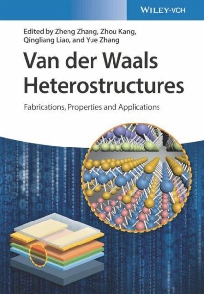
This book systematically introduces the latest developments made in van der Waals heterostructures and devices based on 2D materials in all aspects, from basic synthesis to physical analysis, heterostructures assembling to devices applications.
Andere Kunden interessierten sich auch für
- Yang XuGraphene for Post-Moore Silicon Optoelectronics98,99 €
- Juras BanysVan der Waals Ferroelectrics149,00 €
- Zhigang ZangMetal Oxide Semiconductors95,99 €
- Graphene Field-Effect Transistors122,99 €
- Nanomembranes180,56 €
- Sodium-Ion Capacitors95,99 €
- Manfred FiebigNonlinear Optics on Ferroic Materials103,99 €
-
-
-
This book systematically introduces the latest developments made in van der Waals heterostructures and devices based on 2D materials in all aspects, from basic synthesis to physical analysis, heterostructures assembling to devices applications.
Produktdetails
- Produktdetails
- Verlag: Wiley-VCH
- Artikelnr. des Verlages: 1134950 000
- 1. Auflage
- Seitenzahl: 336
- Erscheinungstermin: 1. März 2023
- Englisch
- Abmessung: 246mm x 174mm x 20mm
- Gewicht: 782g
- ISBN-13: 9783527349500
- ISBN-10: 3527349502
- Artikelnr.: 63896581
- Verlag: Wiley-VCH
- Artikelnr. des Verlages: 1134950 000
- 1. Auflage
- Seitenzahl: 336
- Erscheinungstermin: 1. März 2023
- Englisch
- Abmessung: 246mm x 174mm x 20mm
- Gewicht: 782g
- ISBN-13: 9783527349500
- ISBN-10: 3527349502
- Artikelnr.: 63896581
Dr. Yue Zhang is the academician of Chinese academic society and a full professor of material physics at University of Science and Technology Beijing, China. He has committed to make systematic and innovative contributions to low-dimensional semiconductor materials, functional nanodevices, and nanoscale failure and service behaviors. He has authored over 400 scientific publications and has been nominated as the chief scientist of Major National Scientific Research Projects in China. He won the second prize of the national award for natural sciences. Dr. Zheng Zhang currently is associated professor of School of materials science and engineering in the University of Science and Technology Beijing. His research mainly focuses on two-dimensional atomic crystal materials, nanoelectronics and optoelectronic devices and Low dimensional nano material energy converters. He has published more than 100 peer-reviewed articles in international journals with H-index 35. Qingliang Liao received his Ph.D. degree from University of Science and Technology Beijing (USTB) in 2009. Now he is a professor at Academy for Advanced and Interdisciplinary Science and Technology in USTB. His scientific interests focus on synthesis and characterization of low-dimensional nanomaterials, design and application of functional nanodevices. He has published more than 170 papers in high-quality journals, and has been cited more than 6000 times. He applied for more than 60 national invention patents, and has obtained more than 30 authorized patents. He participated in the writing of 2 English monographs, and his research results have been widely recognized by domestic and foreign counterparts. In addition, he also serves as the editorial board member of 4 international academic journals. Zhuo Kang received his B.S. (2011) and Ph.D. degree (2016) from School of Materials Science and Engineering at University of Science and Technology Beijing (USTB). He is currently a full professor of Material Physics at USTB. His research interests include controllable synthesis and interface engineering of nanomaterials as well as their applications in energy conversion and catalysis, specifically focusing on the efficient modulation of service behaviors under multifield coupling condition and lifetime dynamic structure-performance correlations of electrocatalysts under the service environment.
1 THE 2D SEMICONDUCTOR LIBRARY
1.1 Introduction
1.2. Emerging 2DLMs for Future Electronics
2 THE 2D SEMICONDUCTOR SYNTHESIS AND PERFORMANCES
2.1 Exfoliation
2.2 Chemical Vapor Deposition
3 THE VDW HETEROSTRUCTURE CONTROLLABLE FABRICATIONS
3.1 Wet Transfer
3.2 Controllable Selective Synthesis
3.3 Dry Transfer
4 THE MIXED-DIMENSIONAL VDW HETEROSTRUCTURES
4.1 Categorization of Mixed-dimensional VdWHs
4.2 Strategies for Constructing Mixed-dimensional VdWHs
4.3 Electronic and Sensing Applications
4.4 Optoelectronic and Photonic Applications
4.5 Energy Applications
4.6 Conclusions
5 THE VDW HETEROSTRUCTURE INTERFACE PHYSICS
5.1 Band Alignment and Charge Transfer in VdWHs
5.2 Magnetic Coupling in VdWHs
5.3 Moiré Pattern
5.4 VdWHs for Protection
5.5 Characterization Techniques for VdWHs
6THE VDW HETEROSTRUCTURE MULTI-FIELD COUPLING EFFECTS
6.1 Introduction
6.2 The Multi-Field Coupling Effect Characterization for 2D Van der Waals Structures
6.3 The Multi-Field Modulation for Electrical Properties of 2D Van der Waals Structures
6.4 The Multi-Field Modulation for Optical Properties of 2D Van der Waals Structures
7 VDW HETEROSTRUCTURE ELECTRONICS
7.1 Van der Waals PN Junctions
7.2 Van der Waals Metal-semiconductor Junctions
7.3 Field-effect Transistor
7.4 Junction Field Effect Transistor
7.5 Tunneling Field-effect Transistor
7.6 Van der Waals Integration
8 VDW HETEROSTRUCTURE OPTOELECTRONICS
8.1 Photodetectors
8.2 Light Emission
8.3 Optical Modulators
9 VDW HETEROSTRUCTURE ELECTROCHEMICAL APPLICATIONS
9.1 Solar Energy
9.2 Van der Waals Heterostructure Application on Hydrogen Energy
9.3 Battery
9.4 Catalyst
9.5 Biotechnology
10 PERSPECTIVE AND OUTLOOK
10.1 Overall Development Status of 2D Materials
10.2 Compatibility between 2D van der Waals device processing and silicon technology
10.3. Promising Roadmap of Van der Waals heterostructure devices [Medium term: 5 years, Long term: 5-10 years]
10.4 Promising Roadmap of Optoelectronic Device
10.5 Conclusion and Prospect