136,95 €
136,95 €
inkl. MwSt.
Sofort per Download lieferbar
payback
68 °P sammeln
136,95 €
136,95 €
inkl. MwSt.
Sofort per Download lieferbar

Alle Infos zum eBook verschenken
payback
68 °P sammeln
Als Download kaufen
136,95 €
inkl. MwSt.
Sofort per Download lieferbar
payback
68 °P sammeln
Jetzt verschenken
136,95 €
inkl. MwSt.
Sofort per Download lieferbar

Alle Infos zum eBook verschenken
payback
68 °P sammeln
  • Format: ePub

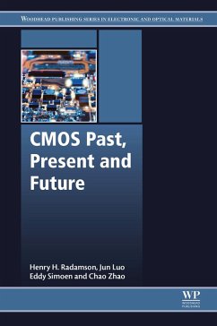
CMOS Past, Present and Future provides insight from the basics, to the state-of-the-art of CMOS processing and electrical characterization, including the integration of Group IV semiconductors-based photonics. The book goes into the pitfalls and opportunities associated with the use of hetero-epitaxy on silicon with strain engineering and the integration of photonics and high-mobility channels on a silicon platform. It begins with the basic definitions and equations, but extends to present technologies and challenges, creating a roadmap on the origins of the technology and its evolution to…mehr

Produktbeschreibung
CMOS Past, Present and Future provides insight from the basics, to the state-of-the-art of CMOS processing and electrical characterization, including the integration of Group IV semiconductors-based photonics. The book goes into the pitfalls and opportunities associated with the use of hetero-epitaxy on silicon with strain engineering and the integration of photonics and high-mobility channels on a silicon platform. It begins with the basic definitions and equations, but extends to present technologies and challenges, creating a roadmap on the origins of the technology and its evolution to the present, along with a vision for future trends.

The book examines the challenges and opportunities that materials beyond silicon provide, including a close look at high-k materials and metal gate, strain engineering, channel material and mobility, and contacts. The book's key approach is on characterizations, device processing and electrical measurements.

  • Addresses challenges and opportunities for the use of CMOS
  • Covers the latest methods of strain engineering, materials integration to increase mobility, nano-scaled transistor processing, and integration of CMOS with photonic components
  • Provides a look at the evolution of CMOS technology, including the origins of the technology, current status and future possibilities

Dieser Download kann aus rechtlichen Gründen nur mit Rechnungsadresse in A, B, BG, CY, CZ, D, DK, EW, E, FIN, F, GR, HR, H, IRL, I, LT, L, LR, M, NL, PL, P, R, S, SLO, SK ausgeliefert werden.

Autorenporträt
Henry H. Radamson received an M.Sc. degree in physics and the Ph.D. degree in semiconductor materials from Linköping University in Sweden, in 1989 and 1996, respectively. In 1997, he joined the Royal Institute of Technology in Stockholm as a senior scientist, where he has been an Associate Professor since 2001.