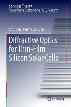
This thesis introduces a figure of merit for light trapping with photonic nanostructures and shows how different light trapping methods compare, irrespective of material, absorber thickness or type of nanostructure. It provides an overview of the essential aspects of light trapping, offering a solid basis for future designs.
Light trapping with photonic nanostructures is a powerful method of increasing the absorption in thin film solar cells. Many light trapping methods have been studied, but to date there has been no comprehensive figure of merit to compare these different methods quantitatively. This comparison allows us to establish important design rules for highly performing structures; one such rule is the structuring of the absorber layer from both sides, for which the authors introduce a novel and simple layer-transfer technique. A closely related issue is the question of plasmonic vs. dielectric nanostructures; the authors present an experimentaldemonstration, aided by a detailed theoretical assessment, highlighting the importance of considering the multipass nature of light trapping in a thin film, which is an essential effect that has been neglected in previous work and which allows us to quantify the parasitic losses.
Dieser Download kann aus rechtlichen Gründen nur mit Rechnungsadresse in A, B, BG, CY, CZ, D, DK, EW, E, FIN, F, GR, HR, H, IRL, I, LT, L, LR, M, NL, PL, P, R, S, SLO, SK ausgeliefert werden.

