
Alle Infos zum eBook verschenken

- Format: PDF
- Merkliste
- Auf die Merkliste
- Bewerten Bewerten
- Teilen
- Produkt teilen
- Produkterinnerung
- Produkterinnerung

Hier können Sie sich einloggen

Bitte loggen Sie sich zunächst in Ihr Kundenkonto ein oder registrieren Sie sich bei bücher.de, um das eBook-Abo tolino select nutzen zu können.
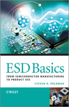
Electrostatic discharge (ESD) continues to impact semiconductor manufacturing, semiconductor components and systems, as technologies scale from micro- to nano electronics. This book introduces the fundamentals of ESD, electrical overstress (EOS), electromagnetic interference (EMI), electromagnetic compatibility (EMC), and latchup, as well as provides a coherent overview of the semiconductor manufacturing environment and the final system assembly. It provides an illuminating look into the integration of ESD protection networks followed by examples in specific technologies, circuits, and chips.…mehr
- Geräte: PC
- mit Kopierschutz
- eBook Hilfe
- Größe: 5.95MB
![ESD (eBook, PDF) ESD (eBook, PDF)]() Steven H. VoldmanESD (eBook, PDF)99,99 €
Steven H. VoldmanESD (eBook, PDF)99,99 €![ESD (eBook, PDF) ESD (eBook, PDF)]() Steven H. VoldmanESD (eBook, PDF)103,99 €
Steven H. VoldmanESD (eBook, PDF)103,99 €![ESD (eBook, PDF) ESD (eBook, PDF)]() Steven H. VoldmanESD (eBook, PDF)116,99 €
Steven H. VoldmanESD (eBook, PDF)116,99 €![The ESD Control Program Handbook (eBook, PDF) The ESD Control Program Handbook (eBook, PDF)]() Jeremy M. SmallwoodThe ESD Control Program Handbook (eBook, PDF)125,99 €
Jeremy M. SmallwoodThe ESD Control Program Handbook (eBook, PDF)125,99 €![Phase-Lock Basics (eBook, PDF) Phase-Lock Basics (eBook, PDF)]() William F. EganPhase-Lock Basics (eBook, PDF)136,99 €
William F. EganPhase-Lock Basics (eBook, PDF)136,99 €![Vertical 3D Memory Technologies (eBook, PDF) Vertical 3D Memory Technologies (eBook, PDF)]() Betty PrinceVertical 3D Memory Technologies (eBook, PDF)95,99 €
Betty PrinceVertical 3D Memory Technologies (eBook, PDF)95,99 €![ESD Basics (eBook, ePUB) ESD Basics (eBook, ePUB)]() Steven H. VoldmanESD Basics (eBook, ePUB)84,99 €
Steven H. VoldmanESD Basics (eBook, ePUB)84,99 €-
-
-
Dieser Download kann aus rechtlichen Gründen nur mit Rechnungsadresse in A, B, BG, CY, CZ, D, DK, EW, E, FIN, F, GR, HR, H, IRL, I, LT, L, LR, M, NL, PL, P, R, S, SLO, SK ausgeliefert werden.
- Produktdetails
- Verlag: John Wiley & Sons
- Seitenzahl: 250
- Erscheinungstermin: 23. August 2012
- Englisch
- ISBN-13: 9781118443279
- Artikelnr.: 37341524
- Verlag: John Wiley & Sons
- Seitenzahl: 250
- Erscheinungstermin: 23. August 2012
- Englisch
- ISBN-13: 9781118443279
- Artikelnr.: 37341524
- Herstellerkennzeichnung Die Herstellerinformationen sind derzeit nicht verfügbar.
Preface xv
Acknowledgments xvii
1 Fundamentals of Electrostatics 1
1.1 Introduction 1
1.2 Electrostatics 1
1.2.1 Thales of Miletus and Electrostatic Attraction 2
1.2.2 Electrostatics and the Triboelectric Series 3
1.2.3 Triboelectric Series and Gilbert 4
1.2.4 Triboelectric Series and Gray 4
1.2.5 Triboelectric Series and Dufay 4
1.2.6 Triboelectric Series and Franklin 5
1.2.7 Electrostatics - Symmer and the Human Body Model 5
1.2.8 Electrostatics - Coulomb and Cavendish 5
1.2.9 Electrostatics - Faraday and the Ice Pail Experiment 5
1.2.10 Electrostatics - Faraday and Maxwell 6
1.2.11 Electrostatics - Paschen 6
1.2.12 Electrostatics - Stoney and the "Electron" 6
1.3 Triboelectric Charging - How does it Happen? 7
1.4 Conductors, Semiconductors, and Insulators 8
1.5 Static Dissipative Materials 8
1.6 ESD and Materials 9
1.7 Electrification and Coulomb's Law 9
1.7.1 Electrification by Friction 10
1.7.2 Electrification by Induction 10
1.7.3 Electrification by Conduction 10
1.8 Electromagnetism and Electrodynamics 11
1.9 Electrical Breakdown 11
1.9.1 Electrostatic Discharge and Breakdown 11
1.9.2 Breakdown and Paschen's Law 12
1.9.3 Breakdown and Townsend 12
1.9.4 Breakdown and Toepler's Law 13
1.9.5 Avalanche Breakdown 13
1.10 Electroquasistatics and Magnetoquasistatics 15
1.11 Electrodynamics and Maxwell's Equations 16
1.12 Electrostatic Discharge (ESD) 16
1.13 Electromagnetic Compatibility (EMC) 16
1.14 Electromagnetic Interference (EMI) 16
1.15 Summary and Closing Comments 17
References 17
2 Fundamentals of Manufacturing and Electrostatics 21
2.1 Materials, Tooling, Human Factors, and Electrostatic Discharge 22
2.1.1 Materials and Human Induced Electric Fields 23
2.2 Manufacturing Environment and Tooling 23
2.3 Manufacturing Equipment and ESD Manufacturing Problems 23
2.4 Manufacturing Materials 24
2.5 Measurement and Test Equipment 24
2.5.1 Manufacturing Testing for Compliance 25
2.6 Grounding and Bonding Systems 27
2.7 Worksurfaces 27
2.8 Wrist Straps 28
2.9 Constant Monitors 28
2.10 Footwear 28
2.11 Floors 28
2.12 Personnel Grounding with Garments 29
2.12.1 Garments 29
2.13 Air Ionization 29
2.14 Seating 29
2.15 Carts 30
2.16 Packaging and Shipping 31
2.16.1 Shipping Tubes 31
2.16.2 Trays 32
2.17 ESD Identification 32
2.18 ESD Program Management - Twelve Steps to Building an ESD Strategy 32
2.19 ESD Program Auditing 33
2.20 ESD On-Chip Protection 33
2.21 Summary and Closing Comments 34
References 34
3 ESD, EOS, EMI, EMC and Latchup 39
3.1 ESD, EOS, EMI, EMC and Latchup 39
3.1.1 ESD 39
3.1.2 EOS 40
3.1.3 EMI 40
3.1.4 EMC 41
3.1.5 Latchup 41
3.2 ESD Models 41
3.2.1 Human Body Model (HBM) 41
3.2.2 Machine Model (MM) 43
3.2.3 Cassette Model 45
3.2.4 Charged Device Model (CDM) 46
3.2.5 Transmission Line Pulse (TLP) 46
3.2.6 Very Fast Transmission Line Pulse (VF-TLP) 50
3.3 Electrical Overstress (EOS) 50
3.3.1 EOS Sources - Lightning 51
3.3.2 EOS Sources - Electromagnetic Pulse (EMP) 52
3.3.3 EOS Sources - Machinery 52
3.3.4 EOS Sources - Power Distribution 52
3.3.5 EOS Sources - Switches, Relays and Coils 53
3.3.6 EOS Design Flow and Product Definition 53
3.3.7 EOS Sources - Design Issues 54
3.3.8 EOS Failure Mechanisms 55
3.4 EMI 57
3.5 EMC 57
3.6 Latchup 58
3.7 Summary and Closing Comments 59
References 59
4 System Level ESD 65
4.1 System Level Testing 65
4.1.1 System Level Testing Objectives 66
4.1.2 Distinction of System and Component Level Testing Failure Criteria 66
4.2 When Systems and Chips Interact 67
4.3 ESD and System Level Failures 68
4.3.1 ESD Current and System Level Failures 68
4.3.2 ESD Induced E- and H-Fields and System Level Failures 69
4.4 Electronic Systems 70
4.4.1 Cards and Boards 70
4.4.2 System Chassis and Shielding 71
4.5 System Level Problems Today 71
4.5.1 Hand Held Systems 71
4.5.2 Cell Phones 71
4.5.3 Servers and Cables 72
4.5.4 Laptops and Cables 74
4.5.5 Disk Drives 74
4.5.6 Digital Cameras 75
4.6 Automobiles, ESD, EOS, and EMI 77
4.6.1 Automobiles and ESD - Ignition Systems 77
4.6.2 Automobiles and EMI - Electronic Pedal Assemblies 77
4.6.3 Automobiles and Gas Tank Fires 78
4.6.4 Hybrids and Electric Cars 78
4.6.5 Automobiles in the Future 79
4.7 Aerospace Applications 80
4.7.1 Airplanes, Partial Discharge, and Lightning 80
4.7.2 Satellites, Spacecraft Charging, and Single Event Upset (SEU) 81
4.7.3 Space Landing Missions 81
4.8 ESD and System Level Test Models 83
4.9 IEC 61000-4-2 83
4.10 Human Metal Model (HMM) 83
4.11 Charged Board Model (CBM) 86
4.12 Cable Discharge Event (CDE) 87
4.12.1 Cable Discharge Event (CDE) and Scaling 89
4.12.2 Cable Discharge Event (CDE) - Cable Measurement Equipment 89
4.12.3 Cable Configuration - Test Configuration 92
4.12.4 Cable Configuration - Floating Cable 92
4.12.5 Cable Configuration - Held Cable 92
4.12.6 Cable Discharge Event (CDE) - Peak Current vs. Charged Voltage 92
4.12.7 Cable Discharge Event (CDE) - Plateau Current vs Charged Voltage 92
4.13 Summary and Closing Comments 93
References 93
5 Component Level Issues - Problems and Solutions 97
5.1 ESD Chip Protection - The Problem and the Cure 97
5.2 ESD Chip Level Design Solutions - Basics of Design Synthesis 98
5.2.1 ESD Circuits 101
5.2.2 ESD Signal Pin Protection Networks 101
5.2.3 ESD Power Clamp Protection Networks 103
5.2.4 ESD Power Domain-to-Domain Circuitry 103
5.2.5 ESD Internal Signal Line Domain-to-Domain Protection Circuitry 104
5.3 ESD Chip Floor Planning - Basics of Design Layout and Synthesis 105
5.3.1 Placement of ESD Signal Pin HBM Circuitry 106
5.3.2 Placement of ESD Signal Pin CDM Circuitry 107
5.3.3 Placement of ESD Power Clamp Circuitry 107
5.3.4 Placement of ESD VSS-to-VSS Circuitry 109
5.4 ESD Analog Circuit Design 109
5.4.1 Symmetry and Common Centroid Design for ESD Analog Circuits 110
5.4.2 Analog Signal Pin to Power Rail ESD Network 111
5.4.3 Common Centroid Analog Signal Pin to Power Rail ESD Network 111
5.4.4 Co-synthesis of Common Centroid Analog Circuit and ESD Networks 112
5.4.5 Signal Pin-to-Signal Pin Differential Pair ESD Network 113
5.4.6 Common Centroid Signal Pin Differential Pair ESD Protection 113
5.5 ESD Radio Frequency (RF) Design 115
5.5.1 ESD Radio Frequency (RF) Design Practices 115
5.5.2 ESD RF Circuits - Signal Pin ESD Networks 121
5.5.3 ESD RF Circuits - ESD Power Clamps 123
5.5.4 ESD RF Circuits - ESD RF VSS-to-VSS Networks 126
5.6 Summary and Closing Comments 127
References 127
6 ESD in Systems - Problems and Solutions 129
6.1 ESD System Solutions from Largest to Smallest 129
6.2 Aerospace Solutions 129
6.3 Oil Tanker Solutions 130
6.4 Automobile Solutions 130
6.5 Computers - Servers 131
6.5.1 Servers - Touch Pads and Handling Procedures 131
6.6 Mother Boards and Cards 131
6.6.1 System Card Insertion Contacts 131
6.6.2 System Level Board Design - Ground Design 131
6.7 System Level "On Board" ESD Protection 133
6.7.1 Spark Gaps 134
6.7.2 Field Emission Devices (FED) 136
6.8 System Level Transient Solutions 140
6.8.1 Transient Voltage Suppression (TVS) Devices 141
6.8.2 Polymer Voltage Suppression (PVS) Devices 143
6.9 Package-Level Mechanical ESD Solutions - Mechanical "Crowbars" 144
6.10 Disk Drive ESD Solutions 145
6.10.1 In Line "ESD Shunt" 145
6.10.2 Armature - Mechanical "Shunt" - A Built-In Electrical "Crowbar" 145
6.11 Semiconductor Chip Level Solutions - Floor Planning, Layout, and
Architecture 147
6.11.1 Mixed Signal Analog and Digital Floor Planning 147
6.11.2 Bipolar-CMOS-DMOS (BCD) Floor Planning 148
6.11.3 System-on Chip Design Floor Planning 148
6.12 Semiconductor Chip Solutions - Electrical Power Grid Design 149
6.12.1 HMM and IEC Specification Power Grid and Interconnect Design
Considerations 150
6.12.2 ESD Power Clamp Design Synthesis - IEC 61000-4-2 Responsive ESD
Power Clamps 151
6.13 ESD and EMC - When Chips Bring Down Systems 152
6.14 System Level and Component Level ESD Testing and System Level Response
152
6.14.1 Time Domain Reflection (TDR) and Impedance Methodology for ESD
Testing 152
6.14.2 Time Domain Reflectometry (TDR) ESD Test System Evaluation 154
6.14.3 ESD Degradation System Level Method - Eye Tests 158
6.15 EMC and ESD Scanning 160
6.16 Summary and Closing Comments 163
References 164
7 Electrostatic Discharge (ESD) in the Future 167
7.1 What is in the Future for ESD? 167
7.2 Factories and Manufacturing 167
7.3 Photo-Masks and Reticles 168
7.3.1 ESD Concerns in Photo-Masks 169
7.3.2 Avalanche Breakdown in Photo-Masks 170
7.3.3 Electrical Model in Photo-Masks 171
7.3.4 Failure Defects in Photo-Masks 172
7.4 Magnetic Recording Technology 174
7.5 Micro-Electromechanical (MEM) Devices 176
7.5.1 ESD Concerns in Micro-Electromechanical (MEM) Devices 177
7.6 Micro-Motors 178
7.6.1 ESD Concerns in Micro-Motors 178
7.7 Micro-Electromechanical (MEM) RF Switches 180
7.7.1 ESD Concerns in Micro-Electromechanical (MEM) RF Switches 180
7.8 Micro-Electromechanical (MEM) Mirrors 182
7.8.1 ESD Concerns in Micro-Electromechanical (MEM) Mirrors 182
7.9 Transistors 183
7.9.1 Transistors - Bulk vs. SOI Technology 184
7.9.2 Transistors and FinFETs 185
7.9.3 ESD in FinFETs 185
7.10 Silicon Nanowires 187
7.11 Carbon Nanotubes 187
7.12 Future Systems and System Designs 188
7.13 Summary and Closing Comments 189
References 190
Glossary 195
ESD Standards 199
Index 203
