Alle Infos zum eBook verschenken
- Format: PDF
- Merkliste
- Auf die Merkliste
- Bewerten Bewerten
- Teilen
- Produkt teilen
- Produkterinnerung
- Produkterinnerung
Hier können Sie sich einloggen
Bitte loggen Sie sich zunächst in Ihr Kundenkonto ein oder registrieren Sie sich bei bücher.de, um das eBook-Abo tolino select nutzen zu können.
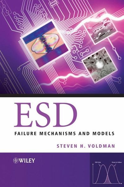
Electrostatic discharge (ESD) failure mechanisms continue to impact semiconductor components and systems as technologies scale from micro- to nano-electronics. This book studies electrical overstress, ESD, and latchup from a failure analysis and case-study approach. It provides a clear insight into the physics of failure from a generalist perspective, followed by investigation of failure mechanisms in specific technologies, circuits, and systems. The book is unique in covering both the failure mechanism and the practical solutions to fix the problem from either a technology or circuit…mehr
- Geräte: PC
- mit Kopierschutz
- eBook Hilfe
- Größe: 6.83MB
- Chris J. MyersAsynchronous Circuit Design (eBook, PDF)152,99 €
- Sami FranssilaIntroduction to Microfabrication (eBook, PDF)67,99 €
- Wolfgang RanklSmart Card Handbook (eBook, PDF)125,99 €
- Steven H. VoldmanESD (eBook, PDF)103,99 €
- Apostolos GeorgiadisMicrowave and Millimeter Wave Circuits and Systems (eBook, PDF)114,99 €
- David J. KinnimentSynchronization and Arbitration in Digital Systems (eBook, PDF)107,99 €
- Arya BehzadWireless LAN Radios (eBook, PDF)101,99 €
-
-
-
Dieser Download kann aus rechtlichen Gründen nur mit Rechnungsadresse in A, B, BG, CY, CZ, D, DK, EW, E, FIN, F, GR, HR, H, IRL, I, LT, L, LR, M, NL, PL, P, R, S, SLO, SK ausgeliefert werden.
- Produktdetails
- Verlag: John Wiley & Sons
- Seitenzahl: 408
- Erscheinungstermin: 1. Juli 2009
- Englisch
- ISBN-13: 9780470747261
- Artikelnr.: 37298987
- Verlag: John Wiley & Sons
- Seitenzahl: 408
- Erscheinungstermin: 1. Juli 2009
- Englisch
- ISBN-13: 9780470747261
- Artikelnr.: 37298987
- Herstellerkennzeichnung Die Herstellerinformationen sind derzeit nicht verfügbar.
Preface.
Acknowledgments.
1 Failure Analysis and ESD.
1.1 Introduction.
1.2 ESD Failure: How Do Micro-electronic Devices Fail?.
1.3 Sensitivity of Semiconductor Components.
1.4 How Do Semiconductor Chips Fail--Are the Failures Random or
Systematic?.
1.5 Closing Comments and Summary.
Problems.
References.
2 Failure Analysis Tools, Models, and Physics of Failure.
2.1 FA Techniques for Evaluation of ESD Events.
2.2 FA Tools.
2.3 ESD Simulation: ESD Pulse Models.
2.4 Electro-Thermal Physical Models.
2.5 Statistical Models for ESD Prediction.
2.6 Closing Comments and Summary.
Problems.
References.
3 CMOS Failure Mechanisms.
3.1 Tables of CMOS ESD Failure Mechanisms.
3.2 LOCOS Isolation-Defined CMOS.
3.3 Shallow Trench Isolation (STI).
3.4 Polysilicon-Defined Devices.
3.5 Lateral Diode with Block Mask.
3.6 MOSFETs.
3.7 Resistors.
3.8 Interconnects: Wires, Vias, and Contacts.
3.9 ESD Failure in CMOS Nanostructures.
3.10 Closing Comments and Summary.
Problems.
References.
4 CMOS Circuits: Receivers and Off-Chip Drivers.
4.1 Tables of CMOS Receiver and OCD ESD Failure Mechanisms.
4.2 Receiver Circuits.
4.3 Receivers Circuits with ESD Networks.
4.4 Receiver Circuits with Half-Pass Transmission Gate.
4.5 Receiver with Full-Pass Transmission Gate.
4.6 Receiver, Half-Pass Transmission Gate, and Keeper Network.
4.7 Receiver Circuit with Pseudo-zero VT Half-Pass Transmission Gate.
4.8 Receiver with Zero VT Transmission Gate.
4.9 Receiver Circuits with Bleed Transistors.
4.10 Receiver Circuits with Test Functions.
4.11 Receiver with Schmitt Trigger Feedback Networks.
4.12 Off-Chip Drivers.
4.13 Single NFET Pull-down OCD.
4.14 Series Cascode MOSFETs.
4.15 I/O Design Considerations and ESD Parasitic Failure Mechanisms.
4.16 Closing Comments and Summary.
Problems.
References.
5 CMOS Integration.
5.1 Table of CMOS Integration ESD Failure Mechanisms.
5.2 Architecture and Design Synthesis-Related Failures.
5.3 Alternate Current Loop.
5.4 Chip Capacitance.
5.5 ESD Power Clamps.
5.6 Intra- and Inter-domain ESD Protection.
5.7 Split Ground Configurations.
5.8 Mixed Voltage Interface.
5.9 Mixed Signal Interface.
5.10 Inter-domain Signal Line ESD Failures.
5.11 Decoupling Capacitors.
5.12 System Clock and Phase-Locked Loop.
5.13 Fuse Networks.
5.14 Bond Pads.
5.15 MOSFET Gate Structure.
5.16 Fill Shapes.
5.17 No Connects.
5.18 Test Circuitry.
5.19 Multi-chip Systems.
5.20 CMOS Latchup Failures.
5.21 Closing Comments and Summary.
Problems.
References.
6 SOI ESD Failure Mechanisms.
6.1 Tables of SOI Device and Integration ESD Failure Mechanisms.
6.2 SOI N-channel MOSFETs.
6.3 SOI Diodes.
6.4 SOI Buried Resistors.
6.5 SOI Failure Mechanisms in 150 nm Technology.
6.6 SOI ESD Failure Mechanisms in 45 nm Technology.
6.7 SOI ESD Failure Mechanisms in 32 nm Technology.
6.8 SOI ESD Failure Mechanisms in 22 nm Technology and the Future.
6.9 SOI Design Synthesis and ESD Failure Mechanisms.
6.10 SOI Integration: ESD Failure Mechanisms.
6.11 Closing Comments and Summary.
Problems.
References.
7 RF CMOS and ESD.
7.1 Tables of RF CMOS ESD Failure Mechanisms.
7.2 RF MOSFET.
7.3 RF Shallow Trench Isolation Diode.
7.4 RF Polysilicon Gated Diode.
7.5 Silicon-Controlled Rectifier.
7.6 Schottky Barrier Diodes.
7.7 Capacitors.
7.8 Resistors.
7.9 Inductors.
7.10 Examples of RF ESD Circuit Failure Mechanisms.
7.11 Closing Comments and Summary.
Problems.
Reference.
8 Micro-electromechanical Systems.
8.1 Table of MEM Failure Mechanisms.
8.2 Electrostatically Actuated Devices.
8.3 Micro-mechanical Engines.
8.4 Torsional Ratcheting Actuator.
8.5 Electromagnetic Micro-power Generators.
8.6 MEM Inductors.
8.7 Electrostatically Actuated Variable Capacitor.
8.8 Micro-mechanical Switches.
8.9 RF MEM Switch.
8.10 Micro-mechanical Mirrors.
8.11 Electrostatically Actuated Torsional Micro-mirrors.
8.12 Closing Comments and Summary.
Problems.
References.
9 Gallium Arsenide.
9.1 Tables of GaAs-Based ESD Failure Mechanisms.
9.2 GaAs Technology.
9.3 GaAs Energy-to-failure and Power-to-failure.
9.4 GaAs ESD Failures in Active and Passive Elements.
9.5 GaAs HBT Devices.
9.6 GaAs HBT-Based Passive Elements.
9.7 GaAs PHEMT Devices.
9.8 GaAs Power Amplifiers.
9.9 InGaAs.
9.10 Gallium Nitride.
9.11 InP and ESD.
9.12 Closing Comments and Summary.
Problems.
References.
10 Smart Power, LDMOS, and BCD Technology.
10.1 Tables of LDMOS ESD Failure Mechanisms.
10.2 LOCOS-Defined LDMOS Devices.
10.3 STI-Defined LDMOS Devices.
10.4 STI-Defined Isolated LDMOS Transistors.
10.5 LDMOS Transistors: ESD Electrical Measurements.
10.6 LDMOS-Based ESD Networks.
10.7 LDMOS ESD Failure Mechanisms.
10.8 LDMOS Transistor Design Enhancement.
10.9 Latchup Events in LDMOS and BCD Technology.
10.10 Closing Comments and Summary.
Problems.
References.
11 Magnetic Recording.
11.1 Tables of Magnetic Recording Failure Mechanisms.
11.2 MR Heads.
11.3 Inductive Heads.
11.4 GMR Heads.
11.5 TMR Heads.
11.6 ESD Solutions.
11.7 Closing Comments and Summary.
Problems.
References.
12 Photo-masks and Reticles: Failure Mechanisms.
12.1 Table of Photo-masks ESD Failure Mechanisms.
12.2 Photo-mask Failure Mechanisms.
12.3 Photo-mask Inspection Tools.
12.4 Photo-mask ESD Characterization.
12.5 Electrical Breakdown Versus Gap Spacing.
12.6 Electrical Breakdown in Air: The Townsend Model.
12.7 Electric Breakdown in Air: Toepler's Spark Law.
12.8 Air Breakdown: The Paschen Breakdown Model.
12.9 Paschen Curve Versus Reticle Breakdown Plot.
12.10 Electrical Model of Photo-mask Breakdown.
12.11 ESD Latent Damage.
12.12 ESD Damage for Single Versus Multiple Events.
12.13 ESD Damage to Anti-reflective Coating.
12.14 ESD Solutions in Photo-masks.
12.15 Closing Comments and Summary.
Problems.
References.
Index.