137,95 €
137,95 €
inkl. MwSt.
Sofort per Download lieferbar
payback
69 °P sammeln
137,95 €
137,95 €
inkl. MwSt.
Sofort per Download lieferbar

Alle Infos zum eBook verschenken
payback
69 °P sammeln
Als Download kaufen
137,95 €
inkl. MwSt.
Sofort per Download lieferbar
payback
69 °P sammeln
Jetzt verschenken
137,95 €
inkl. MwSt.
Sofort per Download lieferbar

Alle Infos zum eBook verschenken
payback
69 °P sammeln
  • Format: PDF

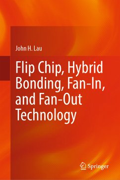
This book focuses on the design, materials, process, fabrication, and reliability of flip chip, hybrid bonding, fan-in, and fan-out technology. Both principles and engineering practice have been addressed, with more weight placed on engineering practice. This is achieved by providing in-depth study on a number of major topics such as wafer bumping, flip chip assembly, underfill and reliability, chip-to-wafer, wafer-to-wafer, Cu-Cu hybrid bonding, WLCSP, 6-side molded WLCSP, FOWLP such as hybrid substrates with PID, ABF, and ultra-large organic interposer, the communications between chiplets…mehr

  • Geräte: PC
  • ohne Kopierschutz
  • eBook Hilfe
  • Größe: 32.24MB
Produktbeschreibung
This book focuses on the design, materials, process, fabrication, and reliability of flip chip, hybrid bonding, fan-in, and fan-out technology. Both principles and engineering practice have been addressed, with more weight placed on engineering practice. This is achieved by providing in-depth study on a number of major topics such as wafer bumping, flip chip assembly, underfill and reliability, chip-to-wafer, wafer-to-wafer, Cu-Cu hybrid bonding, WLCSP, 6-side molded WLCSP, FOWLP such as hybrid substrates with PID, ABF, and ultra-large organic interposer, the communications between chiplets and heterogeneous integration packaging, and on-board optics, near-package optics, and co-packaged optics.

The book benefits researchers, engineers, and graduate students in the fields of electrical engineering, mechanical engineering, materials sciences, industry engineering, etc.


Dieser Download kann aus rechtlichen Gründen nur mit Rechnungsadresse in A, B, BG, CY, CZ, D, DK, EW, E, FIN, F, GR, HR, H, IRL, I, LT, L, LR, M, NL, PL, P, R, S, SLO, SK ausgeliefert werden.

Autorenporträt
John H. Lau, Ph.D., P.E., from July 2019 to June 2021, was the CTO of Unimicron, Taoyuan, Taiwan, where he has been a Senior Special Project Assistant since July 2021. Prior to that, he was a Senior Scientist/MTS with the Hewlett-Packard Laboratory and Agilent, Palo Alto, CA, USA, for 20 years; the Director of the System Packaging Laboratory, Institute of Microelectronics, Singapore, for two years; a Visiting Professor with The Hong Kong University of Science and Technology, Hong Kong, for one year; a Specialist with the Industrial Technology Research Institute, Hsinchu, Taiwan, for five year; a senior technical advisor at ASM Pacific Technology in Hong Kong for five years. He earned a Ph.D. degree in theoretical and applied mechanics from the University of Illinois at Urbana-Champaign. With more than 40 years of R&D and manufacturing experience, he has authored or coauthored more than 530 peer-reviewed technical publications (385 are the principalinvestigator), invented more than 52 issued or pending US patents (31 are the principal inventor), and given more than 350 lectures/workshops/keynotes worldwide. He has authored or coauthored 23 textbooks on fan-out wafer-level packaging, 3D IC heterogeneous integration and packaging, TSV for 3D integration, advanced MEMS packaging, chiplet design and heterogeneous integrated packaging, reliability of 2D and 3D IC interconnects, flip chip, WLP, MCM, area-array packages, WLCSP, high-density PCB, SMT, DCA, TAB, lead-free materials, soldering, manufacturing, and solder joint reliability.