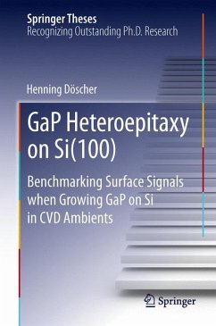
Epitaxial integration of III-V semiconductors on silicon substrates has been desired over decades for high application potential in microelectronics, photovoltaics, and beyond. The performance of optoelectronic devices is still severely impaired by critical defect mechanisms driven by the crucial polar-on-nonpolar heterointerface. This thesis reports almost lattice-matched growth of thin gallium phosphide films as a viable model system for III-V/Si(100) interface investigations. The impact of antiphase disorder on the heteroepitaxial growth surface provides quantitative optical in situ access to one of the most notorious defect mechanisms, even in the vapor phase ambient common for compound semiconductor technology. Precise control over the surface structure of the Si(100) substrates prior to III-V nucleation prevents the formation of antiphase domains. The hydrogen-based process ambient enables the preparation of anomalous double-layer step structures on Si(100), highly beneficial for subsequent III-V integration.
Dieser Download kann aus rechtlichen Gründen nur mit Rechnungsadresse in A, B, BG, CY, CZ, D, DK, EW, E, FIN, F, GR, HR, H, IRL, I, LT, L, LR, M, NL, PL, P, R, S, SLO, SK ausgeliefert werden.


