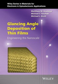
Glancing Angle Deposition of Thin Films (eBook, PDF)
Engineering the Nanoscale
Alle Infos zum eBook verschenken
Glancing Angle Deposition of Thin Films (eBook, PDF)
Engineering the Nanoscale
- Format: PDF
- Merkliste
- Auf die Merkliste
- Bewerten Bewerten
- Teilen
- Produkt teilen
- Produkterinnerung
- Produkterinnerung
Hier können Sie sich einloggen
Bitte loggen Sie sich zunächst in Ihr Kundenkonto ein oder registrieren Sie sich bei bücher.de, um das eBook-Abo tolino select nutzen zu können.
This book provides a highly practical treatment of Glancing Angle Deposition (GLAD), a thin film fabrication technology optimized to produce precise nanostructures from a wide range of materials. GLAD provides an elegant method for fabricating arrays of nanoscale helices, chevrons, columns, and other porous thin film architectures using physical vapour deposition processes such as sputtering or evaporation. The book gathers existing procedures, methodologies, and experimental designs into a single, cohesive volume which will be useful both as a ready reference for those in the field and as a…mehr
- Geräte: PC
- mit Kopierschutz
- eBook Hilfe
- Größe: 17.93MB
- Matthew M. HawkeyeGlancing Angle Deposition of Thin Films (eBook, ePUB)114,99 €
- Atomic Layer Deposition of Nanostructured Materials (eBook, PDF)156,99 €
- Integration of Ferroelectric and Piezoelectric Thin Films (eBook, PDF)201,99 €
- Pulsed Laser Deposition of Thin Films (eBook, PDF)217,99 €
- Tommi KääriäinenAtomic Layer Deposition (eBook, PDF)188,99 €
- Valeri P. TolstoyHandbook of Infrared Spectroscopy of Ultrathin Films (eBook, PDF)407,99 €
- Atomic Layer Deposition of Nanostructured Materials (eBook, ePUB)156,99 €
-
-
-
Dieser Download kann aus rechtlichen Gründen nur mit Rechnungsadresse in A, B, BG, CY, CZ, D, DK, EW, E, FIN, F, GR, HR, H, IRL, I, LT, L, LR, M, NL, PL, P, R, S, SLO, SK ausgeliefert werden.
- Produktdetails
- Verlag: John Wiley & Sons
- Seitenzahl: 320
- Erscheinungstermin: 30. Juni 2014
- Englisch
- ISBN-13: 9781118847329
- Artikelnr.: 41141823
- Verlag: John Wiley & Sons
- Seitenzahl: 320
- Erscheinungstermin: 30. Juni 2014
- Englisch
- ISBN-13: 9781118847329
- Artikelnr.: 41141823
- Herstellerkennzeichnung Die Herstellerinformationen sind derzeit nicht verfügbar.
41 2.4.1 Controlling microstructure and porosity 41 2.4.2 Directional column growth: column tilt ß 44 2.5 Engineering film morphology: column steering via
rotation 47 2.5.1 Controlling column architecture with
: helical columns 47 2.5.2 Controlling microstructure with rotation speed: vertical columns 48 2.5.3 Continuous versus discrete substrate rotation 49 2.6 Growth characteristics of glancing angle deposition technology films 53 2.6.1 Evolutionary column growth 53 2.6.2 Column broadening 56 2.6.3 Column bifurcation 57 2.6.4 Anisotropic shadowing and column fanning 59 2.7 Advanced column steering algorithms 60 2.7.1 ß variations in zigzag microstructures 61 2.7.2 Spin-pause/two-phase substrate rotation: decoupling ß and film density 63 2.7.3 Phisweep motion: competition-resilient structure growth 67 2.8 Additional control over film growth and structure 72 2.8.1 High-temperature glancing angle deposition growth 72 2.8.2 Multimaterial structures: co-deposition processes 75 3 Creating High-Uniformity Nanostructure Arrays 81 3.1 Introduction 81 3.2 Seed layer design 82 3.2.1 Seed spacing and seed height 84 3.2.2 Seed lattice geometry 86 3.2.3 Seed size 87 3.2.4 Planar fill fraction 89 3.2.5 Seed shape 90 3.2.6 Two-dimensional shadow coverage 91 3.2.7 Seed material 94 3.2.8 Design parameter summary 95 3.3 Seed fabrication 95 3.3.1 Conventional techniques 96 3.3.2 Unconventional techniques 97 3.4 Advanced control of local shadowing environment 99 3.4.1 Preventing bifurcation: slow-corner motion 99 3.4.2 Preventing broadening: phisweep and substrate swing 102 4 Properties and Characterization Methods 113 4.1 Introduction 113 4.2 Structural analysis with electron microscopy 113 4.2.1 Practical aspects 114 4.2.2 Scanning electron microscope image analysis 117 4.2.3 Three-dimensional column imaging: tomographic sectioning 122 4.2.4 Characterizing internal column structure with transmission electron microscope imaging 124 4.3 Structural properties of glancing angle deposition films 126 4.3.1 Film surface roughness and evolution 126 4.3.2 Column broadening 128 4.3.3 Intercolumn spacing and column density 133 4.4 Film density 134 4.4.1 Controlling density with
: theoretical models 135 4.4.2 Experimental measurement and control of film density 136 4.5 Porosimetry and surface area determination 140 4.5.1 Surface area enhancement in glancing angle deposition films 141 4.5.2 The pore structure of glancing angle deposition films 144 4.6 Crystallographic texture and evolution 146 4.7 Electrical properties 148 4.7.1 Resistivity in microstructured glancing angle deposition films 148 4.7.2 Anisotropic resistivity 151 4.7.3 Modelling glancing angle deposition film resistivity 153 4.7.4 Individual nanocolumn properties 154 4.8 Mechanical properties 155 4.8.1
effects on film stress 155 4.8.2 Hardness properties 158 4.8.3 Elastic behaviour of glancing angle deposition films 159 4.8.4 Additional mechanical properties 163 5 Glancing Angle Deposition Optical Films 173 5.1 Introduction 173 5.2 The optics of structured glancing angle deposition films 173 5.2.1 Optical anisotropy in columnar glancing angle deposition films 173 5.2.2 Modelling glancing angle deposition films with effective medium theory 176 5.2.3 The column and void material refractive indices 179 5.2.4 Modelling form birefringence via the depolarization factor 180 5.2.5 Dealing with microstructural uncertainty: bounds on the effective dielectric function 182 5.3 Calibrating optical properties of glancing angle deposition films 182 5.3.1 Basic measurements: isotropic approximations 183 5.3.2 Calibrating anisotropy with polarization-sensitive measurements 185 5.3.3 In-depth characterization with generalized techniques 186 5.3.4 Additional factors 186 5.4 Controlling glancing angle deposition film optical properties 187 5.4.1 Basic refractive index engineering with
187 5.4.2 Controlling planar birefringence with
188 5.4.3 Optimizing birefringence with serial bideposition 189 5.4.4 Modulating birefringence with complex
motions 192 5.4.5 Controlling n with advanced glancing angle deposition motions 195 5.5 Graded-index coatings: design and fabrication 195 5.5.1 General design method for glancing angle deposition graded-index coatings 196 5.5.2 Designing
motions for high-accuracy graded-index coatings 197 5.5.3 Specific examples 199 5.5.4 Antireflection coatings 199 5.5.5 Rugate interference filters 201 5.5.6 Avoiding high-
growth instabilities in graded-index films 205 5.6 Designing helical structures for circular polarization optics 206 5.6.1 Optics of chiral glancing angle deposition media 206 5.6.2 Engineering basic helical structures 208 5.6.3 Polygonal helical structures 210 5.6.4 Optimization of circular bragg phenomena with serial bideposition 212 5.6.5 Microcavity design in helical structures 213 5.6.6 Fabricating graded-birefringence thin-film designs 214 5.7 Practical information and issues 216 5.7.1 Post-deposition tuning 216 5.7.2 Environmental sensitivity 217 5.7.3 Optical scattering 217 6 Post-Deposition Processing and Device Integration 227 6.1 Introduction 227 6.2 Post-deposition structural control 227 6.2.1 Annealing 227 6.2.2 Chemical composition control 231 6.2.3 Microstructural control via chemical etching 231 6.2.4 Ion-milling structural modification 233 6.2.5 Column surface modifications 235 6.3 Deposition onto nonplanar geometries 236 6.4 Photolithographic patterning of glancing angle deposition thin films 237 6.5 Encapsulation and replanarization of glancing angle deposition films 240 6.5.1 Encapsulation layer substrate motions 240 6.5.2 Film stress in encapsulation layers 242 6.6 Integrating electrical contacts with glancing angle deposition microstructures 244 6.6.1 Planar electrode configurations 244 6.6.2 Parallel-plate electrode configurations 245 6.7 Films in liquid environments 247 6.8 Using glancing angle deposition microstructures as replication templates 251 6.8.1 Single- and double-template fabrication processes 251 6.8.2 Nanotube fabrication via template fabrication 252 7 Glancing Angle Deposition Systems and Hardware 261 7.1 Introduction 261 7.2 Vacuum conditions 261 7.2.1 Vacuum requirements for glancing angle deposition systems 261 7.2.2 Physical vapour deposition process gases and higher pressure deposition 263 7.3 Thickness calibration and deposition rate monitoring 265 7.3.1 Source directionality and tooling factor 265 7.3.2 Thickness calibration at nonzero
: deposition ratios 267 7.3.3 Extended source: effect on collimation 269 7.4 Uniformity calculations for glancing angle deposition processes 270 7.4.1 Calculating geometry variation over a wafer 270 7.4.2 Mapping out thickness variation 272 7.4.3 Calculating parameter variations for moving substrates 274 7.4.4 Calculating thickness uniformity for moving substrates 276 7.4.5 Calculating column orientation uniformity 278 7.5 Substrate motion hardware 281 7.5.1
motion accuracy and precision 281 7.5.2
motion requirements 283 7.5.3 Additional factors to consider 284 7.5.4 Substrate heating and cooling approaches 285 7.6 Scalability to manufacturing 286 References 286 A Selected Patents 289 Index 297