Sie sind bereits eingeloggt. Klicken Sie auf 2. tolino select Abo, um fortzufahren.
Bitte loggen Sie sich zunächst in Ihr Kundenkonto ein oder registrieren Sie sich bei bücher.de, um das eBook-Abo tolino select nutzen zu können.
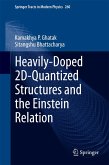
This book highlights the importance of Electron Statistics (ES), which occupies a singular position in the arena of solid state sciences, in heavily doped (HD) nanostructures by applying Heisenberg’s Uncertainty Principle directly without using the complicated Density-of-States function approach as given in the literature. The materials considered are HD quantum confined nonlinear optical, III-V, II-VI, IV-VI, GaP, Ge, PtSb2, stressed materials, GaSb, Te, II-V, Bi2Te3, lead germanium telluride, zinc and cadmium diphosphides, and quantum confined III-V, IV-VI, II-VI and HgTe/CdTe super-lattices…mehr
This book highlights the importance of Electron Statistics (ES), which occupies a singular position in the arena of solid state sciences, in heavily doped (HD) nanostructures by applying Heisenberg’s Uncertainty Principle directly without using the complicated Density-of-States function approach as given in the literature. The materials considered are HD quantum confined nonlinear optical, III-V, II-VI, IV-VI, GaP, Ge, PtSb2, stressed materials, GaSb, Te, II-V, Bi2Te3, lead germanium telluride, zinc and cadmium diphosphides, and quantum confined III-V, IV-VI, II-VI and HgTe/CdTe super-lattices with graded interfaces and effective mass super-lattices. The presence of intense light waves in optoelectronics and strong electric field in nano-devices change the band structure of materials in fundamental ways, which have also been incorporated in the study of ES in HD quantized structures of optoelectronic compounds that control the studies of the HD quantum effect devices under strong fields. The influence of magnetic quantization, magneto size quantization, quantum wells, wires and dots, crossed electric and quantizing fields, intense electric field, and light waves on the ES in HD quantized structures and superlattices are discussed. The content of this book finds six different applications in the arena of nano-science and nanotechnology and the various ES dependent electronic quantities, namely the effective mass, the screening length, the Einstein relation and the elastic constants have been investigated. This book is useful for researchers, engineers and professionals in the fields of Applied Sciences, solid state and materials science, nano-science and technology, condensed matter physics, and allied fields, including courses in semiconductor nanostructures.
Prof. Dr. Engg. Kamakhya Prasad Ghatak of IEM, Kolkata obtained his PhD Degree from the Institute of Radio Physics and Electronics of the Calcutta University in 1988 on the basis of 27 research papers in reputed SCI Journals which is still a record of the said Institute. He is the first Doctor of Engineering Degree awardee of Jadavpur University in 1991(h-index-35, i-10 index- 181& T.C.-5746, the author of 370 SCOPUS publications, 17 books on Nano Technology) and as per World Ranking of top 2% Scientists as prepared by Stanford University, USA, in 2020, he stays within top 1% in the field of Applied Physics. From the position of Assistant Professor in Calcutta University in 1983 up to Senior Professor in the Institute of Engineering and Management, Kolkata in 2015 he was at the top of the merit lists in all the cases. His score in Vidwan portal unit of Government of India is 8.7 out of 10, the highest score among the private Engineering Universities and Institutions of West Bengal. He has produced more than 50 PhD students and the list includes Director, Vice Chancellor, Professors and CEO’s of different Private organization.
Dr. Madhuchhanda Mitra received her Ph.D. from the University of Calcutta, India. She is a recipient of “Griffith Memorial Award” of the University of Calcutta. Her present research interests are nano-science and technology, identification of different biomarkers and biomedical signal processing which includes feature extraction, compression, encryption and classification of electrocardiography (ECG) and photoplethysmography (PPG) signals. At present, she is a professor in the Department of Applied Physics, University of Calcutta, India, where she has been actively engaged in both teaching and research in Instrumentation.
Dr. Arindam Biswas received his M.Tech. in Radio Physics and Electronics from the University of Calcutta, India, in 2010, and Ph.D. from NIT Durgapur, in 2013. He was a postdoctoral researcher at Pusan National University, South Korea, under the prestigious BK21PLUS Fellowship. He was a visiting professor at Research Institute of Electronics, Shizuoka University, Japan. Currently, Dr. Biswas is working as an assistant professor in the School of Mines and Metallurgy, Kazi Nazrul University, Asansol, West Bengal, India. His research interests are in the area of carrier transport in low-dimensional systems and electronic devices, nonlinear optical communications, and THz semiconductor sources.
Inhaltsangabe
1. Introduction.- 2. The HUP and the ES in HD Kane Type III-V and Opto-Electronic Materials Under Intense Electric Field.- 3. The HUP and the ES in Quantum Wells (QWs) of HD Non-Parabolic Materials.- 4. The HUP and the ES in Nano Wires of HD Non-Parabolic Materials.- 5. The HUP and the ES in Quantum Dots (QDs) of HD Non-Parabolic Materials.- 6. The HUP and the ES in doping super lattices of HD Non-Parabolic Semiconductors.- 7. The HUP and the ES in Accumulation Layers of Non-Parabolic Semiconductors.- 8. The HUP and the ES in Heavily Doped (HD) Non-Parabolic Semiconductors under Magnetic quantization.
Es gelten unsere Allgemeinen Geschäftsbedingungen: www.buecher.de/agb
Impressum
www.buecher.de ist ein Internetauftritt der buecher.de internetstores GmbH
Geschäftsführung: Monica Sawhney | Roland Kölbl | Günter Hilger
Sitz der Gesellschaft: Batheyer Straße 115 - 117, 58099 Hagen
Postanschrift: Bürgermeister-Wegele-Str. 12, 86167 Augsburg
Amtsgericht Hagen HRB 13257
Steuernummer: 321/5800/1497