96,29 €
inkl. MwSt.
Sofort per Download lieferbar
  • Format: PDF

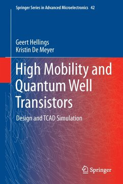
For many decades, the semiconductor industry has miniaturized transistors, delivering increased computing power to consumers at decreased cost. However, mere transistor downsizing does no longer provide the same improvements. One interesting option to further improve transistor characteristics is to use high mobility materials such as germanium and III-V materials. However, transistors have to be redesigned in order to fully benefit from these alternative materials.
High Mobility and Quantum Well Transistors: Design and TCAD Simulation investigates planar bulk Germanium pFET technology in
…mehr

Produktbeschreibung
For many decades, the semiconductor industry has miniaturized transistors, delivering increased computing power to consumers at decreased cost. However, mere transistor downsizing does no longer provide the same improvements. One interesting option to further improve transistor characteristics is to use high mobility materials such as germanium and III-V materials. However, transistors have to be redesigned in order to fully benefit from these alternative materials.

High Mobility and Quantum Well Transistors: Design and TCAD Simulation investigates planar bulk Germanium pFET technology in chapters 2-4, focusing on both the fabrication of such a technology and on the process and electrical TCAD simulation. Furthermore, this book shows that Quantum Well based transistors can leverage the benefits of these alternative materials, since they confine the charge carriers to the high-mobility material using a heterostructure. The design and fabrication of one particular transistor structure - the SiGe Implant-Free Quantum Well pFET – is discussed. Electrical testing shows remarkable short-channel performance and prototypes are found to be competitive with a state-of-the-art planar strained-silicon technology. High mobility channels, providing high drive current, and heterostructure confinement, providing good short-channel control, make a promising combination for future technology nodes.
Autorenporträt
Geert Hellings received the B.S. and M.S. degrees in Electrical Engineering from the KU Leuven, Belgium, in 2007. His master thesis was on III-nitride-based UV detectors for space applications. He obtained the PhD degree from the Electrical Engineering Department (ESAT), Integrated Systems Division (INSYS) at the University of Leuven, Belgium. During his PhD, he worked on the integration of high-mobility channel materials for digital logic applications at imec, Leuven, Belgium. He received a Ph.D. grant from the Institute for the Promotion of Innovation through Science and Technology in Flanders (IWT-Vlaanderen), Brussels, Belgium. He won the 2008 IEEE Region 8 Student Paper Contest and received the 2011 imec Scientific Excellence Award. He has authored or co-authored approximately 70 technical papers for publication in journals and presentations at conferences and holds various patents.

Kristin De Meyer M.Sc. (1974), PhD (1979) KULeuven. She was holder of an IBM World Trade Postdoctoral Fellowship at the IBM T. J. Watson Research Center, Yorktown Heights, NY. Currently she is the Director of Doctoral Research in imec. Since October 1986, she has also been a Part-Time Professor with ESAT-INSYS, KUL. She was the Coordinator for IMEC in several EEC projects. Dr. De Meyer is an IIEE fellow ,member of the Belgian Federal Council for Science Policy and (co) author of over 500 publications.