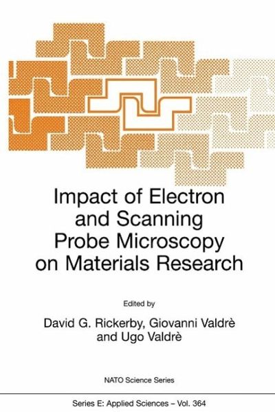
Impact of Electron and Scanning Probe Microscopy on Materials Research (eBook, PDF)
Versandkostenfrei!
Sofort per Download lieferbar
72,95 €
inkl. MwSt.
Weitere Ausgaben:

PAYBACK Punkte
36 °P sammeln!
The Advanced Study Institute provided an opportunity for researchers in universities, industry and National and International Laboratories, from the disciplines ofmaterials science, physics, chemistry and engineering to meet together in an assessment of the impact of electron and scanning probe microscopy on advanced material research. Since these researchers have traditionally relied upon different approaches, due to their different scientific background, to advanced materials problem solving, presentations and discussion within the Institute sessions were initially devoted to developing a se...
The Advanced Study Institute provided an opportunity for researchers in universities, industry and National and International Laboratories, from the disciplines ofmaterials science, physics, chemistry and engineering to meet together in an assessment of the impact of electron and scanning probe microscopy on advanced material research. Since these researchers have traditionally relied upon different approaches, due to their different scientific background, to advanced materials problem solving, presentations and discussion within the Institute sessions were initially devoted to developing a set ofmutually understood basic concepts, inherently related to different techniques ofcharacterization by microscopy and spectroscopy. Particular importance was placed on Electron Energy Loss Spectroscopy (EELS), Scanning Probe Microscopy (SPM), High Resolution Transmission and Scanning Electron Microscopy (HRTEM, HRSTEM) and Environmental Scanning Electron Microscopy (ESEM). It was recognized that the electronic structure derived directly from EELS analysis as well as from atomic positions in HRTEM or High Angle Annular Dark Field STEM can be used to understand the macroscopic behaviour of materials. The emphasis, however, was upon the analysis of the electronic band structure of grain boundaries, fundamental for the understanding of macroscopic quantities such as strength, cohesion, plasticity, etc.
Dieser Download kann aus rechtlichen Gründen nur mit Rechnungsadresse in A, B, BG, CY, CZ, D, DK, EW, E, FIN, F, GR, HR, H, IRL, I, LT, L, LR, M, NL, PL, P, R, S, SLO, SK ausgeliefert werden.


