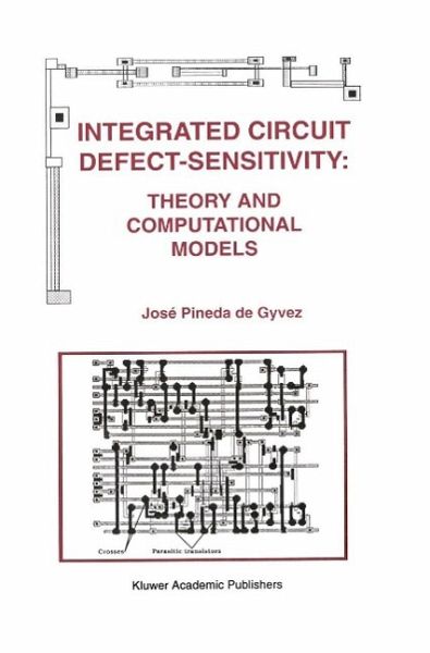
Integrated Circuit Defect-Sensitivity: Theory and Computational Models (eBook, PDF)
Versandkostenfrei!
Sofort per Download lieferbar
72,95 €
inkl. MwSt.
Weitere Ausgaben:

PAYBACK Punkte
36 °P sammeln!
The history of this book begins way back in 1982. At that time a research proposal was filed with the Dutch Foundation for Fundamental Research on Matter concerning research to model defects in the layer structure of integrated circuits. It was projected that the results may be useful for yield estimates, fault statistics and for the design of fault tolerant structures. The reviewers were not in favor of this proposal and it disappeared in the drawers. Shortly afterwards some microelectronics industries realized that their survival may depend on a better integration between technology-and desi...
The history of this book begins way back in 1982. At that time a research proposal was filed with the Dutch Foundation for Fundamental Research on Matter concerning research to model defects in the layer structure of integrated circuits. It was projected that the results may be useful for yield estimates, fault statistics and for the design of fault tolerant structures. The reviewers were not in favor of this proposal and it disappeared in the drawers. Shortly afterwards some microelectronics industries realized that their survival may depend on a better integration between technology-and design-laboratories. For years the "silicon foundry" concept had suggested a fairly rigorous separation between the two areas. The expectation was that many small design companies would share the investment into the extremely costful Silicon fabrication plants while designing large lots of application-specific integrated circuits (ASIC's). Those fabrication plants would be concentrated with only a few market leaders.
Dieser Download kann aus rechtlichen Gründen nur mit Rechnungsadresse in A, B, BG, CY, CZ, D, DK, EW, E, FIN, F, GR, HR, H, IRL, I, LT, L, LR, M, NL, PL, P, R, S, SLO, SK ausgeliefert werden.


