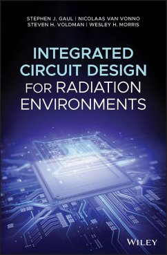
Integrated Circuit Design for Radiation Environments (eBook, ePUB)


Alle Infos zum eBook verschenken

Integrated Circuit Design for Radiation Environments (eBook, ePUB)
- Format: ePub
- Merkliste
- Auf die Merkliste
- Bewerten Bewerten
- Teilen
- Produkt teilen
- Produkterinnerung
- Produkterinnerung

Hier können Sie sich einloggen

Bitte loggen Sie sich zunächst in Ihr Kundenkonto ein oder registrieren Sie sich bei bücher.de, um das eBook-Abo tolino select nutzen zu können.
A practical guide to the effects of radiation on semiconductor components of electronic systems, and techniques for the designing, laying out, and testing of hardened integrated circuits This book teaches the fundamentals of radiation environments and their effects on electronic components, as well as how to design, lay out, and test cost-effective hardened semiconductor chips not only for today's space systems but for commercial terrestrial applications as well. It provides a historical perspective, the fundamental science of radiation, and the basics of semiconductors, as well as…mehr
- Geräte: eReader
- mit Kopierschutz
- eBook Hilfe
- Größe: 19.21MB
![Integrated Circuit Design for Radiation Environments (eBook, PDF) Integrated Circuit Design for Radiation Environments (eBook, PDF)]() Stephen J. GaulIntegrated Circuit Design for Radiation Environments (eBook, PDF)104,99 €
Stephen J. GaulIntegrated Circuit Design for Radiation Environments (eBook, PDF)104,99 €![Design of Power Management Integrated Circuits (eBook, ePUB) Design of Power Management Integrated Circuits (eBook, ePUB)]() Bernhard WichtDesign of Power Management Integrated Circuits (eBook, ePUB)85,99 €
Bernhard WichtDesign of Power Management Integrated Circuits (eBook, ePUB)85,99 €![The ESD Control Program Handbook (eBook, ePUB) The ESD Control Program Handbook (eBook, ePUB)]() Jeremy M. SmallwoodThe ESD Control Program Handbook (eBook, ePUB)125,99 €
Jeremy M. SmallwoodThe ESD Control Program Handbook (eBook, ePUB)125,99 €![75th Anniversary of the Transistor (eBook, ePUB) 75th Anniversary of the Transistor (eBook, ePUB)]() 75th Anniversary of the Transistor (eBook, ePUB)84,99 €
75th Anniversary of the Transistor (eBook, ePUB)84,99 €![The ESD Handbook (eBook, ePUB) The ESD Handbook (eBook, ePUB)]() Steven H. VoldmanThe ESD Handbook (eBook, ePUB)143,99 €
Steven H. VoldmanThe ESD Handbook (eBook, ePUB)143,99 €![MOS Devices for Low-Voltage and Low-Energy Applications (eBook, ePUB) MOS Devices for Low-Voltage and Low-Energy Applications (eBook, ePUB)]() Yasuhisa OmuraMOS Devices for Low-Voltage and Low-Energy Applications (eBook, ePUB)123,99 €
Yasuhisa OmuraMOS Devices for Low-Voltage and Low-Energy Applications (eBook, ePUB)123,99 €![Design of Microwave Active Devices (eBook, ePUB) Design of Microwave Active Devices (eBook, ePUB)]() Design of Microwave Active Devices (eBook, ePUB)144,99 €
Design of Microwave Active Devices (eBook, ePUB)144,99 €-
-
-
Dieser Download kann aus rechtlichen Gründen nur mit Rechnungsadresse in A, B, BG, CY, CZ, D, DK, EW, E, FIN, F, GR, HR, H, IRL, I, LT, L, LR, M, NL, PL, P, R, S, SLO, SK ausgeliefert werden.
- Produktdetails
- Verlag: John Wiley & Sons
- Seitenzahl: 392
- Erscheinungstermin: 3. Dezember 2019
- Englisch
- ISBN-13: 9781118701850
- Artikelnr.: 58421372
- Verlag: John Wiley & Sons
- Seitenzahl: 392
- Erscheinungstermin: 3. Dezember 2019
- Englisch
- ISBN-13: 9781118701850
- Artikelnr.: 58421372
- Herstellerkennzeichnung Die Herstellerinformationen sind derzeit nicht verfügbar.
Centers 120 3.3.2.2 Continuous-Time Random-Walk (CTRW) 122 3.3.3 The Silicon/Silicon Dioxide Interface 124 3.3.3.1 Interface Traps 125 3.3.3.2 Border Traps 127 3.3.3.3 Hydrogen 128 3.3.3.4 ELDRS 130 3.4 Bulk Damage 131 3.5 Summary and Closing Comments 133 References 135 4 Radiation-Induced Single Events 143 4.1 Introduction - Single-Events Effects (SEE) 143 4.1.1 Single-Event Upsets (SEU) 143 4.1.2 Multiple-Bit Upset (MBU) 143 4.1.3 Single-Event Transients (SET) 144 4.1.4 Single-Event Functional Interrupts (SEFIs) 144 4.1.5 Single-Event Disturb (SED) 145 4.1.6 Single-Event Snapback (SESB) 146 4.1.7 Single-Event Latchup (SEL) 146 4.1.8 Single-Event Burnout (SEB) 146 4.1.9 Single-Event Gate Rupture (SEGR) 147 4.1.10 Single-Event Hard Errors (SHE) 147 4.2 Single-Event Upset (SEU) 148 4.2.1 SEU - Memory 148 4.2.2 SEU in CMOS Memory 148 4.2.3 SEU in Bipolar Memory 148 4.2.4 SEU in CMOS SRAM 149 4.2.5 SEU in Future Technology - FINFETs 149 4.3 SEU - Particle Sources 149 4.3.1 SEU Source - Alpha Particles 150 4.3.2 SEU Source - Pions and Muons 152 4.3.3 SEU - Neutrons 153 4.3.4 SEU Source - Protons 153 4.3.5 SEU - Heavy Ions 154 4.4 Single-Event Gate Rupture (SEGR) 154 4.4.1 Definition SEGR 155 4.4.2 SEGR Source - Ion Track 155 4.4.3 SEGR Source - Failure Mechanism 156 4.4.4 SEGR - Modeling and Simulation 156 4.4.5 Power Transistors and SEGR 156 4.4.5.1 Lateral Power Transistors SEGR 156 4.4.5.2 Vertical MOS (VMOS) SEGR 157 4.4.5.3 Advanced Technologies - Planar MOSFET SEGR 157 4.5 Single-Event Transients (SETs) 158 4.5.1 SET Definition 158 4.5.2 SET Source 158 4.5.3 SET Source Failure Mechanisms 159 4.5.4 SET in Integrated Circuits 159 4.5.4.1 Digital Circuitry 159 4.5.4.2 Continuous Time Analog Circuitry 159 4.5.5 Prediction and Hardening 159 4.6 Single-Event Latchup (SEL) 159 4.6.1 SEL Definition 160 4.6.2 SEL Source 160 4.6.3 SEL Time Response 161 4.6.4 SEL Maximum Charge Collection Evaluation in a Parallelepiped Region 162 4.6.5 A SEL Design Practice 164 4.6.6 SEL Semiconductor Device Simulation 165 4.7 Summary and Closing Comments 165 References 166 5 Radiation Testing 173 5.1 Introduction 173 5.1.1 Radiation Units and Measurements 173 5.2 Radiation Testing and Sources 175 5.2.1 Total Ionizing Dose (TID) Testing 176 5.2.2 Total Ionizing Dose (TID) Sources 179 5.2.3 Single-Event Effects (SEE) Testing 182 5.2.4 Single-Event Effects (SEE) Sources and Facilities 187 5.2.5 Neutron Testing 192 5.2.6 Neutron Sources 193 5.2.7 Proton Testing 195 5.2.8 Proton Sources 196 5.2.9 Transient Gamma Testing 197 5.2.10 Transient Gamma Sources 198 5.3 Summary and Closing Comments 201 References 204 6 Device Modeling and Simulation Techniques 209 6.1 Introduction 209 6.2 Device Modeling 210 6.2.1 Circuit Simulators 211 6.2.2 Intrinsic Models 212 6.2.3 Composite Models and Inline Subcircuits 212 6.2.4 Analysis and Statistics Programs 214 6.3 Radiation Effects on Semiconductor Devices 215 6.3.1 MOS Capacitors and Transistors 215 6.3.1.1 MOS Capacitors 216 6.3.1.2 MOS Transistors 219 6.3.2 Diodes and Bipolar Transistors 224 6.3.2.1 Diodes 224 6.3.2.2 Bipolar Transistors 225 6.3.3 Power Devices 230 6.3.3.1 DMOS Composite Models 231 6.3.3.2 Operating Voltage 232 6.3.4 Other Devices 232 6.3.4.1 Junction Field Effect Transistors (JFETs) 232 6.3.4.2 Resistors 234 6.3.4.3 Capacitors 235 6.3.5 Some Modeling Challenges 235 6.4 Circuit Simulation 236 6.4.1 Corner Simulation 236 6.4.2 SEE Simulation 239 6.5 Summary and Closing Comments 242 References 244 7 Radiation Semiconductor Process and Layout Solutions 249 7.1 Introduction 249 7.2 Substrate Hardened Technologies 249 7.2.1 Silicon-on-Insulator (SOI) Technologies 250 7.2.1.1 Separation by Implanted Oxygen (SIMOX) 250 7.2.1.2 Silicon-Bonded (SIBOND) Technology 250 7.2.2 Silicon on Sapphire (SOS) 251 7.2.3 Silicon on Diamond (SOD) 252 7.2.4 Silicon on Nothing (SON) 252 7.3 Oxide Hardening Technologies 253 7.3.1 Oxide Growth and Fluorination of Oxide 253 7.3.2 MOSFET Gate Oxide Hardening 253 7.3.3 Recessed Oxide (ROX) Hardening 254 7.3.4 LOCOS Isolation Hardening 254 7.3.5 Shallow Trench Isolation (STI) Hardening 254 7.4 CMOS Latchup Process Solutions 255 7.5 CMOS Substrates - High-Resistance Substrates 255 7.5.1 50
-cm Substrate Resistance 259 7.6 Wells 260 7.6.1 Single Well - Diffused N-Well 261 7.6.2 Single Well - Retrograde N-Well 261 7.6.3 Dual-Well Technology 262 7.6.3.1 P-well and P++ Substrate 262 7.6.3.2 P-Well and P+ Connecting Implant 263 7.7 Triple-Well Technology 264 7.7.1 Triple Well - Full Separation of Wells 264 7.7.2 Triple Well - Merged Triple Well 265 7.7.3 Triple Well - Merged Triple Well with Blanket Implant 266 7.8 Sub-Collectors 266 7.8.1 Epitaxial Grown Sub-Collector 266 7.8.2 Implanted Sub-Collector 267 7.8.3 Sub-Collector - NPN and PNP Bipolar Current Gain 267 7.8.4 Sub-Collector - Beta Product
PNP
NPN 267 7.9 Heavily Doped Buried Layers (HDBL) 268 7.9.1 Buried Implanted Layer for Lateral Isolation (BILLI) Process 268 7.9.2 Continuous HDBL Implant 268 7.9.3 Buried Guard Ring (BGR) 270 7.10 Isolation Concepts 270 7.10.1 LOCOS Isolation 270 7.10.2 Shallow Trench Isolation (STI) 270 7.10.3 Dual Depth Isolation 271 7.10.4 Trench Isolation (TI) 272 7.10.4.1 Trench Isolation (TI) and Sub-Collector 274 7.11 Deep Trench 277 7.11.1 Deep Trench (DT) within PNPN Structure 279 7.11.2 Deep Trench Structure and Sub-Collector 281 7.11.3 Deep Trench Structure and Merged Triple Well 283 7.12 Layout Solutions 284 7.12.1 Polysilicon Bound Structures 284 7.12.2 Parasitic Isolation Device (PID) 284 7.13 Summary and Closing Comments 286 References 287 8 Single-Event Upset Circuit Solutions 293 8.1 Introduction 293 8.2 CMOS DRAM SEU Circuit Solutions 293 8.2.1 CMOS DRAM Redundancy 294 8.2.2 CMOS DRAM with SRAM Error Correction 294 8.3 CMOS SRAM SEU Circuit Solution 296 8.3.1 CMOS SRAM Four-Device Cell 296 8.3.2 CMOS SRAM Six-Device Cell 297 8.3.3 CMOS SRAM 12-Device Cell 298 8.4 Bipolar SRAM 299 8.4.1 Bipolar SRAM Cell with Resistor Loads 300 8.4.2 Bipolar SRAM Cell with Resistor Loads and Schottky Clamps 300 8.4.3 Bipolar SRAM Cell with PNP Transistors 301 8.5 Bipolar SRAM Circuit Solutions 301 8.6 SEU in CMOS Logic Circuitry 302 8.7 Summary and Closing Comments 302 References 303 9 Latchup Circuit Solutions 305 9.1 Introduction 305 9.2 Power Supply Concepts 305 9.2.1 Power Supply Current Limit - Series Resistor 305 9.2.2 Power Supply Current Limit - Current Source 306 9.2.3 Power Supply Solutions - Voltage Regulator 307 9.2.4 Latchup Circuit Solutions - Power Supply Decoupling 308 9.3 Overshoot and Undershoot Clamp Networks 311 9.3.1 Passive Clamp Networks 312 9.3.2 Active Clamp Networks 313 9.3.3 Dynamic Threshold Triple Well Passive and Active Clamp Networks 316 9.4 Passive and Active Guard Rings 318 9.4.1 Passive Guard Ring Circuits and Structures 318 9.4.2 Active Guard Ring Circuits and Structures 319 9.5 Triple-Well Noise and Latchup Suppression Structures 326 9.6 System-Level Latchup Issues 326 9.7 Summary and Closing Comments 327 References 329 10 Emerging Effects and Future Technology 333 10.1 Introduction 333 10.2 Radiation Effects in Advanced Technologies 333 10.2.1 Moore's Law, Scaling, and Radiation Effects 334 10.2.2 Technology Lifetime and Reliability 334 10.2.2.1 New Missions 335 10.2.2.2 Throwaway Mentality 335 10.2.2.3 New Space Entrants 335 10.2.3 Terrestrial Issues 335 10.2.4 Space Mission Issues 335 10.2.5 Server Farms 335 10.2.6 Automotive 336 10.2.7 Internet of Things (IoT) 336 10.2.8 More than Moore 336 10.3 Radiation Effects in Semiconductor Nanostructures 336 10.3.1 Planar MOSFETs in Sub-25 nm 337 10.3.2 Bulk FinFET 338 10.3.3 SOI FinFET 339 10.3.4 3-D Circuits 340 10.4 Radiation Effects and Advanced Packaging 340 10.4.1 Radiation Effects and 2.5-D Circuits and Technology 341 10.4.2 Radiation Effects and 3-D Circuits and Technology 341 10.4.3 More than Moore and 3-D Integration 342 10.5 Ruggedized Capability 342 10.5.1 Ruggedized Capability for Radiation 343 10.5.2 Ruggedized Capability for High Temperature 343 10.6 Radiation Models 343 10.7 A Nuclear World 344 10.8 Summary and Closing Comments 344 References 345 Index 347


