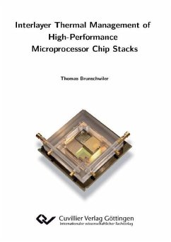
Vertical integration of integrated circuit dies offers tremendous opportunities from an architectural as well as from an economical standpoint. Memory proximity supports performance scaling, and might enable significant energy savings. Partitioning of the corresponding functionalities and technologies into individual tiers can improve yield and modularity substantially.
The paradigm change of stacking active components has a direct impact on heat-removal concepts and is therefore the motivation of this thesis. A stack comprised of a single logic layer in combination with multiple memory dies was identified as the limit for traditional back-side heat removal. To minimize junction temperatures, a stacking sequence with the high heat-flux component in close proximity to the cold plate is proposed.
Interlayer cooling is the only volumetric heat-removal solution that scales with the number of dies in the stack. Hence, the focus of this thesis has been to identify the potential of interlayer cooling and to provide a modeling framework. Fundamental heat-transfer building blocks, such as unit-cell geometries, fluid structure modulation, fluid focusing, as well as four-port fluid delivery supporting power-map-aware heat removal, are discussed. Moreover, the theoretical foundation was experimentally validated on resistively heated convective test cavities. Therefore, specific bonding and insulation schemes were developed. Finally, the interlayer cooling performance was demonstrated on a pyramid chip stack.
A multi-scale modeling approach for the efficient design of non-uniform heat-removal cavities was proposed. Periodic arrangements of heat-removal unit-cells in the cavities are described by the porousmedia approximation. Their characteristics are represented by the directional and velocity-dependent modified permeability and convective thermal resistance. An extended tensor description was developed to map the pressure gradient to the DARCY velocity. These parameters were derived from detailed numerical heat and mass transport modeling for arbitrary angle-of-attack of the fluid, using a set of novel routines that support periodic hydrodynamic and thermal boundary conditions. For pin-fin arrays, a biased fluid flow towards directions with maximal permeability could be observed. Fieldcoupling between the two-dimensional porous and adjacent three-dimensional solid domains was performed to derive the temperature field in the chip stack, including heat spreading in the silicon die. The modeling results are conservative and deviate less than 20% from the measured junction temperatures, when considering the temperature dependency of the coolant viscosity. This is a very good value considering the immense complexity reduction, resulting in a low computational time of less than 20 min on a desktop computer, to derive the mass transport and junction temperatures within a chip stack.
Sputtered AuSn 80/20 was investigated as eutectic thin-film bond to form leak-tight interfaces with mechanical, electrical, and thermal functionality, as part of the technology development, to enable the use of water as coolant. The resulting bond quality was characterized for various underbump metallizations, atmospheres, and reflow/force profiles. The implementation of a differential pumped chamber allowed the use of formic acid in the flip chip bonder to reduce the tin oxide on the solder surface. The transient liquid-solid nature of the thin-film solder process explains the sensitivity on the underbump metallization and the heat ramp. Finally, processing guidelines supporting the design of leak-tight bond interfaces were summarized. Acceptable intermetallic compound formation was achieved at heat ramps of 100 K/min and with chromium as wetting layer. A bondline thickness of 4μm and a Teflon support provided sufficient compliance to form successful bonds considering the wedge errors of the flip chip bonder.
Waterproof, two-level metallizations to mimic processor-like, non-uniform power maps with background and hot-spot heaters were developed for the implementation of single- and multi-cavity test sections. Pin-hole-free dielectric layers (1μm PECVD Si3N4 / 100nm ALD Al2O3) were achieved by conformal thin-film deposition.
Numerous heat transfer assessments yielded the following insights:
The limited heat capacity and flow rate of the coolant were identified as the major contributor to the thermal gradient in convective interlayer heat removal, even when water using as coolant. This is due to the small hydraulic diameter defined by the interconnect density (pitches < 200 μm) and the length of the cross-flow heat exchange cavity ( 10 mm).
The circular pin-fin in-line unit-cell was identified as the optimal heat transfer geometry for heat capacity limited cross-flow heat transfer. It results in the highest porosity, beneficial for efficient mass transport, compared with microchannels and other pin shapes at a given minimal radius constraint. Improved convective heat transfer towards the outlet of the cavities caused by transient vortex shedding was observed at increased REYNOLDS numbers (> 100) in the pin-fin in-line case.
Fluid cavities with four-port fluid delivery and heat removal geometry modulation need to be considered for chip stacks larger than 2 cm2 and a interconnect pitch of 50 μm. Their effectiveness was demonstrated with cavities that were either partially fully or half populated with pin-fin arrays. These arrangements result in a significant increase in local fluid flow compared with uniform heat transfer cavities.
Microchannels have proved to dissipate heat efficiently to multiple fluid cavities in the chip stack because of the improved die-to-die coupling, caused by the 50% fin fill factor. This is advantageous for disparate tier stacking. The high-power die can benefit from heat dissipation into cavities adjacent to low-power tiers.
Additional recommendations, critical for electro-thermal co-design, are also discussed: i) Heat spreading in the silicon helps to mitigate hot-spots below a critical spatial dimension of 1mm. ii) High heat flux macros should be placed towards the fluid inlet and die corners if the two- or four-port configuration is implemented, respectively. iii) A manifold width of 1mm should be considered to achieve a fluid maldistribution below 1% between the fluid cavities. iv) A 1.6 ms thermal time constant was derived for an interlayer cooled chip stack. Hence, predictive cooling-loop control schemes need to be implemented to account for the comparable high pump time constant.
Finally, for the first time, the superiority of interlayer cooling as a volumetric heat-removal method could be experimentally demonstrated on the pyramid chip stack test vehicle with four fluid cavities and three power dissipating tiers. Aligned hot-spots were included with 250 W/cm2 heat flux each. A total power of 390 W, corresponding to a 3.9 kW/cm3 volumetric heat flow, could be dissipated on the 1 cm2 device at a 54.7 K junction temperature increase. In comparison, back-side cooling would result in a junction temperature increase of 223 K with respect to the fluid inlet temperature of the microchannel cold plate. Using the results of the present work, it is now possible to design and predict mass and heat transport in an interlayer cooled chip stack, with the support of the proposed best-practice design rules in combination with the validated multi-scale modeling framework. The scalable nature of interlayer cooling will enable “Extreme-3D-Integration” with computation in sugar cube form factor chip stacks, extending integration density and efficiency scaling beyond the “End-of-2D-Scaling”.
Dieser Download kann aus rechtlichen Gründen nur mit Rechnungsadresse in A, B, BG, CY, CZ, D, DK, EW, E, FIN, F, GR, HR, H, IRL, I, LT, L, LR, M, NL, PL, P, R, S, SLO, SK ausgeliefert werden.


