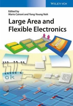
Large Area and Flexible Electronics (eBook, PDF)
Redaktion: Caironi, Mario; Noh, Yong-Young
Alle Infos zum eBook verschenken
Large Area and Flexible Electronics (eBook, PDF)
Redaktion: Caironi, Mario; Noh, Yong-Young
- Format: PDF
- Merkliste
- Auf die Merkliste
- Bewerten Bewerten
- Teilen
- Produkt teilen
- Produkterinnerung
- Produkterinnerung
Hier können Sie sich einloggen
Bitte loggen Sie sich zunächst in Ihr Kundenkonto ein oder registrieren Sie sich bei bücher.de, um das eBook-Abo tolino select nutzen zu können.
From materials to applications, this ready reference covers the entire value chain from fundamentals via processing right up to devices, presenting different approaches to large-area electronics, thus enabling readers to compare materials, properties and performance. Divided into two parts, the first focuses on the materials used for the electronic functionality, covering organic and inorganic semiconductors, including vacuum and solution-processed metal-oxide semiconductors, nanomembranes and nanocrystals, as well as conductors and insulators. The second part reviews the devices and…mehr
- Geräte: PC
- mit Kopierschutz
- eBook Hilfe
- Größe: 16.18MB
Dieser Download kann aus rechtlichen Gründen nur mit Rechnungsadresse in A, B, BG, CY, CZ, D, DK, EW, E, FIN, F, GR, HR, H, IRL, I, LT, L, LR, M, NL, PL, P, R, S, SLO, SK ausgeliefert werden.
- Produktdetails
- Verlag: Wiley-VCH
- Seitenzahl: 558
- Erscheinungstermin: 13. Januar 2014
- Englisch
- ISBN-13: 9783527680009
- Artikelnr.: 42153266
- Verlag: Wiley-VCH
- Seitenzahl: 558
- Erscheinungstermin: 13. Januar 2014
- Englisch
- ISBN-13: 9783527680009
- Artikelnr.: 42153266
- Herstellerkennzeichnung Die Herstellerinformationen sind derzeit nicht verfügbar.
His current research interests are on direct-writing and roll-to-roll printing processes for organic and hybrid micro- and opto-electronics, on the device physics of OFETSs and on organic thermoelectrics.
Yong-Young Noh is Associate Professor in the Department of Energy and Materials Engineering at Dongguk University in Seoul, Republic of Korea. He received his PhD in 2005 from the Gwangju Institute of Science and Technology (GIST), Republic of Korea, and then worked at the Cavendish Laboratory in Cambridge, UK, as a postdoctoral associate with Prof. Henning Sirringhaus from 2005 t0 2007. Afterwards, he worked at the Electronics and Telecommunications Research Institute (ETRI), Republic of Korea, as a senior researcher from 2008 to 2009, and at Hanbat National University as assistant professor from 2010 to 2012. Yong-Young Noh has received Merck Young Scientist Award (2013) and Korea President Award (2014). He has expertise in materials, process and device physics of organic and printed electronics for flexible electronics, especially printed OFETs, carbon nanotube or oxide TFTs and OLEDs.
PART I: Materials
POLYMERIC AND SMALL-MOLECULE SEMICONDUCTORS FOR ORGANIC FIELD-EFFECT TRANSISTORS
Introduction
Organic Semiconductor Structural Design
Thin-Film Transistor Applications
p-Channel Semiconductors
n-Channel Semiconductors
Ambipolar Semiconductors
Conclusions
METAL-OXIDE THIN-FILM TRANSISTORS FOR FLEXIBLE ELECTRONICS
Introduction
Metal-Oxide TFTs
Solution-Processed MO Thin Films
Low-Temperature-Processed MO TFTs for Flexible Electronics
Summary
CARBON NANOTUBE THIN-FILM TRANSISTORS
Introduction
Individual SWCNTs and SWCNT Thin Films
Chemical Vapor Deposition Growth of SWCNT TFTs
Solution-Based Methods for SWCNT TFTs
Inkjet Printing of Flexible SWCNT TFTs
Fabrication Schemes for High-Performance Inkjet-Printed SWCNT TFTs
Inkjet Printing of SWCNT CMOS Inverters
Inkjet Priting of Aligned SWCNT Films
Conclusion
ORGANIC SINGLE-CRYSTALLINE SEMICONDUCTORS FOR FLEXIBLE ELECTRONICS APPLICATIONS
Introduction
Electronic and Structural Properties of Single Crystals
Crystallization Techniques
Single-Crystal Flexible Electronic Devices
Strategies for Flexible Organic Single-Crystal Device Fabrication
Conclusions
SOLUTION-PROCESSABLE QUANTUM DOTS
Introduction
Optimization of the Colloidal Synthesis of Quantum Dots by Selection of Suitable Solvents, Ligands, and Precursors
Large-Scale Synthesis of Quantum Dots
Surface Chemistry of Quantum Dots
Post-Synthetic Chemical Modification of Nanocrystals
Conclusions and Outlook
INORGANIC SEMICONDUCTOR NANOMATERIALS FOR FLEXIBLE ELECTRONICS
Introduction
Characteristics and Synthesis of Inorganic Semiconducting NMs
Applications in Flexible Electronics
Concluding Remarks
DIELECTRIC MATERIALS FOR LARGE-AREA AND FLEXIBLE ELECTRONICS
Introduction
General Polymer Dielectrics
Cross-Linked Polymer Dielectrics
High-k Polymer Dielectrics
Electrolyte Gate Dielectrics
Self-Assembled Molecular Layer Dielectrics
Hybrid Dielectrics
Sol-Gel High-k Inorganic Dielectrics
Summary and Outlook
ELECTROLYTE-GATING ORGANIC THIN FILM TRANSISTORS
Introduction
Electrolyte Gated OTFT Operation Mechanisms
Electrolyte Materials
OTFTs Gated with Electrolyte Dielectrics
Circuits Baed on Electrolyte-Gated OTFTs
Conclusions
VAPOR BARRIER FILMS FOR FLEXIBLE ELECTRONICS
Introduction
Thin-Film Permeation Barrier Layers
Permeation through Inorganic Thin Films
Time-Resolved Measurements on Barrier Layers
Mechanical Limitations of Inorganic Films
Mechanics of Films on Flexible Substrates
Summary
LATEST ADVANCES IN SUBSTRATES FOR FLEXIBLE ELECTRONICS
Introduction
Factors Influencing Film Choice
Film Property Set
Summary of Key Properties of Base Substrates
Planarizing Coatings
Examples of Film in Use
Concluding Remarks
PART II: Devices and Applications
INKJET PRINTING PROCESS FOR LARGE AREA ELECTRONICS
Introduction
Dynamics of Jet Formation
Ink Rheology: Non-Newtonian Liquids
Dynamics of Drop Impact and Spreading
Applications of Inkjet Printing for Large-Area Electronics
Summary
INKJET PRINTED ELECTRONIC CIRCUITS BASED ON ORGANIC SEMICONDUCTORS
Printed Organic Electronics
CMOS Technology
High-Speed Organic CMOS Circuits
Conclusions
LARGE-AREA, PRINTED ORGANIC CIRCUITS FOR AMBIENT ELECTRONICS
Introduction
Manufacturing Process and Electrical Characteristics
Demonstration
Future Prospects
POLYMER AND ORGANIC NONVOLATILE MEMORY DEVICES
Introduction
Resistive Switching Memories
Charge Storage in Transistor Gate Dielectric
Polymer Ferroelectric Devices
Conclusions
FLEXIBLE DISPLAYS
Introduction
Flexible Substrates
Display Mode
Thin-Film Transistor
AMOLED Panel with Printing Technology
Fabrication of the OLED and AMOLED Panel
Future Prospects
FLEXIBLE ORGANIC SOLAR CELLS FOR SCALABLE, LOW-COST PHOTOVOLTAIC ENERGY CONVERSION
Overview of Organic Photovoltaic (OPV) Cells
Efforts toward Realization of Flexible OSCs
Flexible OSCs for High-Throughput Production: A Printing-Based Approach to Low-Cost Solar Energy Conversion
Summary and Outlook
FLEXIBLE INORGANIC PHOTOVOLTAICS
Introduction
Thin Crystalline Solar Cells Transferred onto Flexible Substrates
Thin-Film Solar Cells Grown Directly onto Flexible Substrates by Vapor Deposition
Solution-ProcessedThin-Film Solar Cells Deposited Directly onto Flexible Substrates
Summary
SCALABLE AND FLEXIBLE BIOELECTRONICS AND ITS APPLICATIONS TO MEDICINE
Biosensing and Bioelectronics: A Fast Growing Field and a Challenging Research Area
Inorganic and Silicon-Based Flexible Electronics for Biosensing Devices
EGOFETs for Flexible Biosensing
OECTs for Biosensing and Biomonitoring
Conclusions and Outlook
Index