Sie sind bereits eingeloggt. Klicken Sie auf 2. tolino select Abo, um fortzufahren.
Bitte loggen Sie sich zunächst in Ihr Kundenkonto ein oder registrieren Sie sich bei bücher.de, um das eBook-Abo tolino select nutzen zu können.
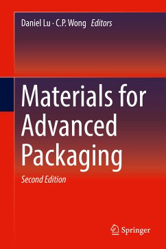
This second edition continues to be the most comprehensive review on the developments in advanced packaging technologies. Experts in the field discuss established techniques, as well as emerging technologies, to provide readers with the most up-to-date developments in advanced packaging. Original chapters on bonding and joining techniques, nanopackaging and biomedical packaging, MEMS and wafer level chip scale packaging, and packaging materials such as lead-free solders, flip chip underfills, epoxy molding compounds, and conductive adhesives have all been updated with the latest developments…mehr
This second edition continues to be the most comprehensive review on the developments in advanced packaging technologies. Experts in the field discuss established techniques, as well as emerging technologies, to provide readers with the most up-to-date developments in advanced packaging. Original chapters on bonding and joining techniques, nanopackaging and biomedical packaging, MEMS and wafer level chip scale packaging, and packaging materials such as lead-free solders, flip chip underfills, epoxy molding compounds, and conductive adhesives have all been updated with the latest developments in the field. New chapters have also been added on fast growing and emerging applications such as flexible and printed electronics, materials solutions to enable next generation thinner/lighter/more functional mobile devices, and functional coating for electronic devices such as anti-fingerprint coating, anti-scratch coating, and more. This book is ideal for professionals in semiconductor, digital health, and bio-medical areas as well as graduate students studying materials science and engineering.
Dr. Daniel Lu is the Vice President of Technology, Henkel Corporation in Asia Pacific. Prior to joining Henkel, he worked for the R&D department of Intel Corp (Arizona, USA) as a Sr. Scientist for 7 years. He received his MS and PhD degrees on Polymer Science and Engineering from Georgia Institute of Technology in 1996 and 2000, respectively. Dr. Lu received many awards including the IEEE/CPMT Outstanding Young Engineer Award in 2004, the IEEE ECTC best poster paper in 2007, Intel’s most patent filing in 2003-2007, etc. Dr. Lu has published more than 50 journal papers, wrote chapters for six books, and holds more than 80 US and international patents. He is the editor of the book “Materials for Advanced Packaging (2008)” and co-author of the book “Electronically Conductive Adhesives with Nanotechnologies (2009)”. He has been serving key roles in organizing international electronic packaging conferences and teaching professional development courses in these conferences. Dr. Lu is a senior member of IEEE, and an associate editor of IEEE Transactions on Advanced Packagingand Journal of Nanomaterials, and an editorial board member of Nanoscience & Nanotechnology-Asia. Dr. Lu also serves as an adjunct professor in Huazhong University of Science and Technology, and SIAT (Shenzhen Institute of Advanced Technologies), Chinese Academy of Science. Dr. Lu has more 15 years of experience in electronic packaging and is an expert in electronic packaging materials and processing.
Professor C.P. Wong is with the School of Materials Sciences and Engineering at Georgia Tech (GT) and also is the Dean of Engineering, The Chinese University of Hong Kong. Prior to joining GT, he was with AT&T Bell Laboratories for many years and was an AT&T Bell Labs Fellow. His research interests focus on the areas of material and process for electronic, photonic, MEMS, sensors, and energy harvesting and storage. He has published over 1,000 technical papers, 12 books and holds over 65 US Patents. He is a member of the US National Academy of Engineering and a Foreign Academician of the Chinese Academy of Engineering.
Inhaltsangabe
3D Integration Technologies – An Overview.- Advanced Bonding/Joining Techniques.- Advanced Chip-to-Substrate Connections.- Advanced Wire Bonding Technology: Materials, Methods, and Testing.- Lead-Free Soldering.- Thin Die Fabrication and Applications to Wafer Level System Integration.- Advanced Substrates: A Materials and Processing Perspective.- Flip-Chip Underfill: Materials, Process and Reliability.- New Development Trend of Epoxy Molding Compound for Encapsulating Semiconductor Chips.- Electrically Conductive Adhesives (ECAs).- Die Attach Adhesives and Films.- Thermal Interface Materials.- Embedded Passives.- Advanced Bonding Technology Based on Nano- and Micro-metal Pastes.- Wafer Level Chip Scale Packaging.- MEMS Packaging.- LED Die Bonding.- Medical Electronics Design, Manufacturing, and Reliability.- Flexible and Printed Electronics.- Silicon Solar Cell Metallization Pastes.- Nano-metal Assisted Chemical Etching for Fabricating Semiconductor and Optoelectronic Devices.- Characterization of Copper Diffusion in Through Silicon Vias.
3D Integration Technologies - An Overview.- Advanced Bonding/Joining Techniques.- Advanced Chip-to-Substrate Connections.- Advanced Wire Bonding Technology: Materials, Methods, and Testing.- Lead-Free Soldering.- Thin Die Fabrication and Applications to Wafer Level System Integration.- Advanced Substrates: A Materials and Processing Perspective.- Flip-Chip Underfill: Materials, Process and Reliability.- New Development Trend of Epoxy Molding Compound for Encapsulating Semiconductor Chips.- Electrically Conductive Adhesives (ECAs).- Die Attach Adhesives and Films.- Thermal Interface Materials.- Embedded Passives.- Advanced Bonding Technology Based on Nano- and Micro-metal Pastes.- Wafer Level Chip Scale Packaging.- MEMS Packaging.- LED Die Bonding.- Medical Electronics Design, Manufacturing, and Reliability.- Flexible and Printed Electronics.- Silicon Solar Cell Metallization Pastes.- Nano-metal Assisted Chemical Etching for Fabricating Semiconductor and Optoelectronic Devices.- Characterization of Copper Diffusion in Through Silicon Vias.
Es gelten unsere Allgemeinen Geschäftsbedingungen: www.buecher.de/agb
Impressum
www.buecher.de ist ein Internetauftritt der buecher.de internetstores GmbH
Geschäftsführung: Monica Sawhney | Roland Kölbl | Günter Hilger
Sitz der Gesellschaft: Batheyer Straße 115 - 117, 58099 Hagen
Postanschrift: Bürgermeister-Wegele-Str. 12, 86167 Augsburg
Amtsgericht Hagen HRB 13257
Steuernummer: 321/5800/1497