158,99 €
158,99 €
inkl. MwSt.
Sofort per Download lieferbar

0 °P sammeln
158,99 €
Als Download kaufen

158,99 €
inkl. MwSt.
Sofort per Download lieferbar

0 °P sammeln
Jetzt verschenken
Alle Infos zum eBook verschenken
158,99 €
inkl. MwSt.
Sofort per Download lieferbar
Alle Infos zum eBook verschenken

0 °P sammeln
- Format: PDF
- Merkliste
- Auf die Merkliste
- Bewerten Bewerten
- Teilen
- Produkt teilen
- Produkterinnerung
- Produkterinnerung

Bitte loggen Sie sich zunächst in Ihr Kundenkonto ein oder registrieren Sie sich bei
bücher.de, um das eBook-Abo tolino select nutzen zu können.
Hier können Sie sich einloggen
Hier können Sie sich einloggen
Sie sind bereits eingeloggt. Klicken Sie auf 2. tolino select Abo, um fortzufahren.

Bitte loggen Sie sich zunächst in Ihr Kundenkonto ein oder registrieren Sie sich bei bücher.de, um das eBook-Abo tolino select nutzen zu können.
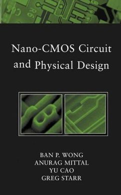
Based on the authors' expansive collection of notes taken over the years, Nano-CMOS Circuit and Physical Design bridges the gap between physical and circuit design and fabrication processing, manufacturability, and yield. This innovative book covers: process technology, including sub-wavelength optical lithography; impact of process scaling on circuit and physical implementation and low power with leaky transistors; and DFM, yield, and the impact of physical implementation.
- Geräte: PC
- mit Kopierschutz
- eBook Hilfe
- Größe: 5.44MB
Andere Kunden interessierten sich auch für
![Nano-CMOS Design for Manufacturability (eBook, PDF) Nano-CMOS Design for Manufacturability (eBook, PDF)]() Ban P. WongNano-CMOS Design for Manufacturability (eBook, PDF)117,99 €
Ban P. WongNano-CMOS Design for Manufacturability (eBook, PDF)117,99 €![Multi-voltage CMOS Circuit Design (eBook, PDF) Multi-voltage CMOS Circuit Design (eBook, PDF)]() Volkan KursunMulti-voltage CMOS Circuit Design (eBook, PDF)110,99 €
Volkan KursunMulti-voltage CMOS Circuit Design (eBook, PDF)110,99 €![Low-Voltage SOI CMOS VLSI Devices and Circuits (eBook, PDF) Low-Voltage SOI CMOS VLSI Devices and Circuits (eBook, PDF)]() James B. KuoLow-Voltage SOI CMOS VLSI Devices and Circuits (eBook, PDF)147,99 €
James B. KuoLow-Voltage SOI CMOS VLSI Devices and Circuits (eBook, PDF)147,99 €![RF Circuit Design (eBook, PDF) RF Circuit Design (eBook, PDF)]() Richard C. LiRF Circuit Design (eBook, PDF)171,99 €
Richard C. LiRF Circuit Design (eBook, PDF)171,99 €![Device Modeling for Analog and RF CMOS Circuit Design (eBook, PDF) Device Modeling for Analog and RF CMOS Circuit Design (eBook, PDF)]() Trond YtterdalDevice Modeling for Analog and RF CMOS Circuit Design (eBook, PDF)147,99 €
Trond YtterdalDevice Modeling for Analog and RF CMOS Circuit Design (eBook, PDF)147,99 €![VLSI Circuit Design Methodology Demystified (eBook, PDF) VLSI Circuit Design Methodology Demystified (eBook, PDF)]() Liming XiuVLSI Circuit Design Methodology Demystified (eBook, PDF)89,99 €
Liming XiuVLSI Circuit Design Methodology Demystified (eBook, PDF)89,99 €![Nano Lithography (eBook, PDF) Nano Lithography (eBook, PDF)]() Nano Lithography (eBook, PDF)139,99 €
Nano Lithography (eBook, PDF)139,99 €-
-
-
Based on the authors' expansive collection of notes taken over the years, Nano-CMOS Circuit and Physical Design bridges the gap between physical and circuit design and fabrication processing, manufacturability, and yield. This innovative book covers: process technology, including sub-wavelength optical lithography; impact of process scaling on circuit and physical implementation and low power with leaky transistors; and DFM, yield, and the impact of physical implementation.
Dieser Download kann aus rechtlichen Gründen nur mit Rechnungsadresse in A, B, BG, CY, CZ, D, DK, EW, E, FIN, F, GR, HR, H, IRL, I, LT, L, LR, M, NL, PL, P, R, S, SLO, SK ausgeliefert werden.
Produktdetails
- Produktdetails
- Verlag: Wiley
- Seitenzahl: 394
- Erscheinungstermin: 8. April 2005
- Englisch
- ISBN-13: 9780471678861
- Artikelnr.: 37359330
- Verlag: Wiley
- Seitenzahl: 394
- Erscheinungstermin: 8. April 2005
- Englisch
- ISBN-13: 9780471678861
- Artikelnr.: 37359330
- Herstellerkennzeichnung Die Herstellerinformationen sind derzeit nicht verfügbar.
BAN P. WONG, IENG MIEE, served for five years as a member of the technical program committee of IEEE International Solid-State Circuits Conference and as session chair, cochair, and organizer of a panel session. He has three issued patents. He has led circuit design teams in developing methodology and implementation of high-performance and low-power microprocessors. He is currently Senior Engineering Manager for NVIDIA Corporation. ANURAG MITTAL received his PhD in applied physics from Yale University. He has codeveloped novel embedded NVM microcontroller and microprocessor solutions including the world's first truly CMOS-compatible Flash technology. He is Senior Staff Engineer for Virage Logic, Inc. YU CAO received his PhD in electrical engineering from University of California, Berkeley. He is a postdoctoral researcher in the Berkeley Wireless Research Center. He received the 2000 Beatrice Winner Award at the IEEE International Solid-State Circuits Conference. GREG STARR received his PhD in electrical engineering from Arizona State University. Currently, he is a Senior Design Manager at Xilinx Corporation.
FOREWORD.
PREFACE.
1 NANO-CMOS SCALING PROBLEMS AND IMPLICATIONS.
1.1 Design Methodology in the Nano-CMOS Era.
1.2 Innovations Needed to Continue Performance Scaling.
1.3 Overview of Sub-100-nm Scaling Challenges and Subwavelength Optical
Lithography.
1.4 Process Control and Reliability.
1.5 Lithographic Issues and Mask Data Explosion.
1.6 New Breed of Circuit and Physical Design Engineers.
1.7 Modeling Challenges.
1.8 Need for Design Methodology Changes.
1.9 Summary.
References.
PART I: PROCESS TECHNOLOGY AND SUBWAVELENGTH OPTICAL LITHOGRAPHY: PHYSICS,
THEORY OF OPERATION, ISSUES, AND SOLUTIONS.
2 CMOS DEVICE AND PROCESS TECHNOLOGY.
2.1 Equipment Requirements for Front-End Processing.
2.2 Front-End-Device Problems in CMOS Scaling.
2.3 Back-End-of-Line Technology.
References.
3 THEORY AND PRACTICALITIES OF SUBWAVELENGTH OPTICAL LITHOGRAPHY.
3.1 Introduction and Simple Imaging Theory.
3.2 Challenges for the 100-nm Node.
3.3 Resolution Enhancement Techniques: Physics.
3.4 Physical Design Style Impact on RET and OPC Complexity.
3.5 The Road Ahead: Future Lithographic Technologies.
References.
PART II: PROCESS SCALING IMPACT ON DESIGN 4 MIXED-SIGNAL CIRCUIT DESIGN.
4.1 Introduction.
4.2 Design Considerations.
4.3 Device Modeling.
4.4 Passive Components.
4.5 Design Methodology.
4.6 Low-Voltage Techniques.
4.7 Design Procedures.
4.8 Electrostatic Discharge Protection.
4.9 Noise Isolation.
4.10 Decoupling.
4.11 Power Busing.
4.12 Integration Problems.
4.13 Summary.
References.
5 ELECTROSTATIC DISCHARGE PROTECTION DESIGN.
5.1 Introduction.
5.2 ESD Standards and Models.
5.3 ESD Protection Design.
5.4 Low-C ESD Protection Design for High-Speed I/O.
5.5 ESD Protection Design for Mixed-Voltage I/O.
5.6 SCR Devices for ESD Protection.
5.7 Summary.
References.
6 INPUT/OUTPUT DESIGN.
6.1 Introduction.
6.2 I/O Standards.
6.3 Signal Transfer.
6.4 ESD Protection.
6.5 I/O Switching Noise.
6.6 Termination.
6.7 Impedance Matching.
6.8 Preemphasis.
6.9 Equalization.
6.10 Conclusion.
References.
7 DRAM.
7.1 Introduction.
7.2 DRAM Basics.
7.3 Scaling the Capacitor.
7.4 Scaling the Array Transistor.
7.5 Scaling the Sense Amplifier.
7.6 Summary.
References.
8 SIGNAL INTEGRITY PROBLEMS IN ON-CHIP INTERCONNECTS.
8.1 Introduction.
8.2 Interconnect Parasitics Extraction.
8.3 Signal Integrity Analysis.
8.4 Design Solutions for Signal Integrity.
8.5 Summary.
References.
9 ULTRALOW POWER CIRCUIT DESIGN.
9.1 Introduction.
9.2 Design-Time Low-Power Techniques.
9.3 Run-Time Low-Power Techniques.
9.4 Technology Innovations for Low-Power Design.
9.5 Perspectives for Future Ultralow-Power Design.
References.
PART III: IMPACT OF PHYSICAL DESIGN ON MANUFACTURING/YIELD AND PERFORMANCE.
10 DESIGN FOR MANUFACTURABILITY.
10.1 Introduction.
10.2 Comparison of Optimal and Suboptimal Layouts.
10.3 Global Route DFM.
10.4 Analog DFM.
10.5 Some Rules of Thumb.
10.6 Summary.
References.
11 DESIGN FOR VARIABILITY.
11.1 Impact of Variations on Future Design.
11.2 Strategies to Mitigate Impact Due to Variations.
11.3 Corner Modeling Methodology for Nano-CMOS Processes.
11.4 New Features of the BSIM4 Model.
11.5 Summary.
References.
INDEX.
