84,95 €
84,95 €
inkl. MwSt.
Sofort per Download lieferbar
payback
0 °P sammeln
84,95 €
84,95 €
inkl. MwSt.
Sofort per Download lieferbar

Alle Infos zum eBook verschenken
payback
0 °P sammeln
Als Download kaufen
84,95 €
inkl. MwSt.
Sofort per Download lieferbar
payback
0 °P sammeln
Jetzt verschenken
84,95 €
inkl. MwSt.
Sofort per Download lieferbar

Alle Infos zum eBook verschenken
payback
0 °P sammeln
  • Format: PDF

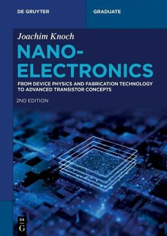
In recent years, nanoelectronics has become very interdisciplinary requiring students to master aspects of physics, electrical engineering, chemistry etc. The 2nd edition of this textbook is a comprehensive overview of nanoelectronics covering the necessary quantum mechanical and solid-state physics foundation, an overview of semiconductor fabrication as well as a brief introduction into device simulation using the non-equilibrium Greens function formalism. Equipped with this, the work discusses nanoscale field-effect transistors and alternative device concepts such as Schottky-barrier MOSFETs…mehr

  • Geräte: PC
  • ohne Kopierschutz
  • eBook Hilfe
  • Größe: 77.68MB
  • FamilySharing(5)
Produktbeschreibung
In recent years, nanoelectronics has become very interdisciplinary requiring students to master aspects of physics, electrical engineering, chemistry etc. The 2nd edition of this textbook is a comprehensive overview of nanoelectronics covering the necessary quantum mechanical and solid-state physics foundation, an overview of semiconductor fabrication as well as a brief introduction into device simulation using the non-equilibrium Greens function formalism. Equipped with this, the work discusses nanoscale field-effect transistors and alternative device concepts such as Schottky-barrier MOSFETs as well as steep slope transistors based on different materials. In addition, cryogenic operation of MOSFETs for the realization of, e.g., classical control electronics of semiconducting spin qubits is studied.

The work contains a number of tasks, examples and exercises with step-by-step video solutions as well as tutorial videos that deepen the understanding of the material. With additional access to simulation tools that allow students to do computational experiments, the emphasis is on thorough explanation of the material enabling students to carry out their own research.

Joachim Knoch studied physics at RWTH Aachen University and Queen Mary, University of London; he obtained the MSc and PhD degrees in physics from RWTH Aachen University in 1998 and 2001, respectively. In his PhD dissertation he worked on the modeling and realization of ultrashort channel silicon MOSFETs. After the PhD, he joined the Microsystem Technology Laboratory, Massachusetts Institute of Technology as a postdoctoral fellow working on InP HEMTs. Between 2003 and 2006 he was a researcher at the Forschungszentrum Jülich in Jülich/Germany where he investigated tunnel FETs as well as Schottky-barrier transistors. In 2006 he accepted a position as research staff member at IBM's Zurich Research Laboratory in Switzerland continuing to study tunnel FETs based on nanowires. He was appointed associate professor of electrical engineering at TU Dortmund University, Dortmund/Germany in 2008 and since 2011 he has been full professor of electrical engineering at RWTH Aachen University. His current research interests cover nanoelectronics devices based on group IV materials as well as 2D materials for low power, cryogenic and neuromorphic applications.


Dieser Download kann aus rechtlichen Gründen nur mit Rechnungsadresse in A, B, BG, CY, CZ, D, DK, EW, E, FIN, F, GR, HR, H, IRL, I, LT, L, LR, M, NL, PL, P, R, S, SLO, SK ausgeliefert werden.

Autorenporträt
Joachim Knoch studied physics at RWTH Aachen University and Queen Mary, University of London; he obtained the MSc and PhD degrees in physics from RWTH Aachen University in 1998 and 2001, respectively. In his PhD dissertation he worked on the modeling and realization of ultrashort channel silicon MOSFETs. After the PhD, he joined the Microsystem Technology Laboratory, Massachusetts Institute of Technology as a postdoctoral fellow working on InP HEMTs. Between 2003 and 2006 he was a researcher at the Forschungszentrum Jülich in Jülich/Germany where he investigated tunnel FETs as well as Schottky-barrier transistors. In 2006 he accepted a position as research staff member at IBM's Zurich Research Laboratory in Switzerland continuing to study tunnel FETs based on nanowires. He was appointed associate professor of electrical engineering at TU Dortmund University, Dortmund/Germany in 2008 and since 2011 he has been full professor of electrical engineering at RWTH Aachen University. His current research interests cover nanoelectronics devices based on group IV materials as well as 2D materials for low power, cryogenic and neuromorphic applications.