81,95 €
81,95 €
inkl. MwSt.
Sofort per Download lieferbar
payback
41 °P sammeln
81,95 €
81,95 €
inkl. MwSt.
Sofort per Download lieferbar

Alle Infos zum eBook verschenken
payback
41 °P sammeln
Als Download kaufen
81,95 €
inkl. MwSt.
Sofort per Download lieferbar
payback
41 °P sammeln
Jetzt verschenken
81,95 €
inkl. MwSt.
Sofort per Download lieferbar

Alle Infos zum eBook verschenken
payback
41 °P sammeln
  • Format: PDF

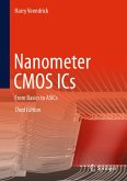
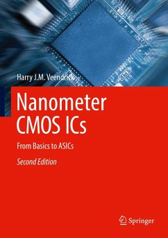
This textbook provides a comprehensive, fully-updated introduction to the essentials of nanometer CMOS integrated circuits. It includes aspects of scaling to even beyond 12nm CMOS technologies and designs. It clearly describes the fundamental CMOS operating principles and presents substantial insight into the various aspects of design implementation and application. Coverage includes all associated disciplines of nanometer CMOS ICs, including physics, lithography, technology, design, memories, VLSI, power consumption, variability, reliability and signal integrity, testing, yield, failure…mehr

  • Geräte: PC
  • ohne Kopierschutz
  • eBook Hilfe
  • Größe: 23.62MB
Produktbeschreibung
This textbook provides a comprehensive, fully-updated introduction to the essentials of nanometer CMOS integrated circuits. It includes aspects of scaling to even beyond 12nm CMOS technologies and designs. It clearly describes the fundamental CMOS operating principles and presents substantial insight into the various aspects of design implementation and application. Coverage includes all associated disciplines of nanometer CMOS ICs, including physics, lithography, technology, design, memories, VLSI, power consumption, variability, reliability and signal integrity, testing, yield, failure analysis, packaging, scaling trends and road blocks. The text is based upon in-house Philips, NXP Semiconductors, Applied Materials, ASML, IMEC, ST-Ericsson, TSMC, etc., courseware, which, to date, has been completed by more than 4500 engineers working in a large variety of related disciplines: architecture, design, test, fabrication process, packaging, failure analysis and software.

Dieser Download kann aus rechtlichen Gründen nur mit Rechnungsadresse in A, B, BG, CY, CZ, D, DK, EW, E, FIN, F, GR, HR, H, IRL, I, LT, L, LR, M, NL, PL, P, R, S, SLO, SK ausgeliefert werden.

Autorenporträt
Harry Veendrick graduated from the Technical University Eindhoven, the Netherlands, in 1977. In the same year he joined Philips Research Laboratories, also in Eindhoven, where he has been involved in the design of memories, gate arrays and complex digital video-signal processors. He holds 30 US and many more European patents in the area of CMOS circuit design, with several other patents pending, and he is the (co-)author of more than 30 publications on robust, high-performance and low-power CMOS IC design. In this respect, he has contributed to many conferences and conference workshops, as reviewer, speaker, invited speaker, panellist, organizer, guest editor and program committee member. In addition, he is the author of MOS ICs (VCH 1992), Deep-Submicron CMOS ICs, from Basics to ASICs (Kluwer Academic Publishers: 1-st edition 1998, 2-nd edition 2000) and Nanometer CMOS ICs, from Basics to ASICs (Springer: 1-st edition June 2008). He is a co-author of Low-Power Electronics Design (CRCPress, 2004). His principle research interests included the design of low-power and high-speed complex digital CMOS circuits, with an emphasis on nanometer-scale physical effects and scaling aspects. From 2002 to 2009 he has been project leader of the Deep-Submicron/Nanometer CMOS Electrical Design Cluster within the research group Mixed-Signal Circuits and Systems at NXP Research, which is the 2006 spin-off of the disentangled former Philips Semiconductors Product and R&D Departments. Complementary to this is his interest in IC technology, which allows him to act as an interface between digital IC design and IC process technology. From 1980 onwards, next to his research activities, he has been actively involved in the training of more than 4500 semiconductor design, test, product, CAD tools and process engineers. In 2002 he received the PhD degree in electronic engineering from the Technical University of Eindhoven, The Netherlands. He was a Research Fellow at Philips Research Laboratories and NXP Research and has been a Visiting Professor to the Department of Electronic and Electrical Engineering of the University of Strathclyde, Glasgow, Scotland, UK. In May 2009 he has left NXP Research and started his own training activity teaching 1-day, 3-day and 5-day courses for different target audiences (NanoCMOS-Training BV).