44,95 €
44,95 €
inkl. MwSt.
Sofort per Download lieferbar

22 °P sammeln
44,95 €
Als Download kaufen

44,95 €
inkl. MwSt.
Sofort per Download lieferbar

22 °P sammeln
Jetzt verschenken
Alle Infos zum eBook verschenken
44,95 €
inkl. MwSt.
Sofort per Download lieferbar
Alle Infos zum eBook verschenken

22 °P sammeln
- Format: PDF
- Merkliste
- Auf die Merkliste
- Bewerten Bewerten
- Teilen
- Produkt teilen
- Produkterinnerung
- Produkterinnerung

Bitte loggen Sie sich zunächst in Ihr Kundenkonto ein oder registrieren Sie sich bei
bücher.de, um das eBook-Abo tolino select nutzen zu können.
Hier können Sie sich einloggen
Hier können Sie sich einloggen
Sie sind bereits eingeloggt. Klicken Sie auf 2. tolino select Abo, um fortzufahren.

Bitte loggen Sie sich zunächst in Ihr Kundenkonto ein oder registrieren Sie sich bei bücher.de, um das eBook-Abo tolino select nutzen zu können.
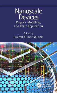
The aim of this book is to discuss various aspects of nanoscale devices design and their applications including transport mechanism, modeling, and circuit applications. Furthermore, the book develops a strong foundation to understand the need for moving from conventional MOSFET to the novel devices.
- Geräte: PC
- mit Kopierschutz
- eBook Hilfe
- Größe: 36.18MB
Andere Kunden interessierten sich auch für
![Introduction to Microelectronics to Nanoelectronics (eBook, PDF) Introduction to Microelectronics to Nanoelectronics (eBook, PDF)]() Manoj Kumar MajumderIntroduction to Microelectronics to Nanoelectronics (eBook, PDF)48,95 €
Manoj Kumar MajumderIntroduction to Microelectronics to Nanoelectronics (eBook, PDF)48,95 €![Introductory Nanoelectronics (eBook, PDF) Introductory Nanoelectronics (eBook, PDF)]() Vinod Kumar KhannaIntroductory Nanoelectronics (eBook, PDF)42,95 €
Vinod Kumar KhannaIntroductory Nanoelectronics (eBook, PDF)42,95 €![Introduction to Spintronics (eBook, PDF) Introduction to Spintronics (eBook, PDF)]() Supriyo BandyopadhyayIntroduction to Spintronics (eBook, PDF)52,95 €
Supriyo BandyopadhyayIntroduction to Spintronics (eBook, PDF)52,95 €![Nanocrystals in Nonvolatile Memory (eBook, PDF) Nanocrystals in Nonvolatile Memory (eBook, PDF)]() Writam BanerjeeNanocrystals in Nonvolatile Memory (eBook, PDF)161,95 €
Writam BanerjeeNanocrystals in Nonvolatile Memory (eBook, PDF)161,95 €![Plasma Electronics (eBook, PDF) Plasma Electronics (eBook, PDF)]() Toshiaki MakabePlasma Electronics (eBook, PDF)78,95 €
Toshiaki MakabePlasma Electronics (eBook, PDF)78,95 €![Meso- to Micro- Actuators (eBook, PDF) Meso- to Micro- Actuators (eBook, PDF)]() Alberto BorboniMeso- to Micro- Actuators (eBook, PDF)53,95 €
Alberto BorboniMeso- to Micro- Actuators (eBook, PDF)53,95 €![Introductory Semiconductor Device Physics (eBook, PDF) Introductory Semiconductor Device Physics (eBook, PDF)]() Greg ParkerIntroductory Semiconductor Device Physics (eBook, PDF)50,95 €
Greg ParkerIntroductory Semiconductor Device Physics (eBook, PDF)50,95 €-
-
-
The aim of this book is to discuss various aspects of nanoscale devices design and their applications including transport mechanism, modeling, and circuit applications. Furthermore, the book develops a strong foundation to understand the need for moving from conventional MOSFET to the novel devices.
Dieser Download kann aus rechtlichen Gründen nur mit Rechnungsadresse in A, B, BG, CY, CZ, D, DK, EW, E, FIN, F, GR, HR, H, IRL, I, LT, L, LR, M, NL, PL, P, R, S, SLO, SK ausgeliefert werden.
Produktdetails
- Produktdetails
- Verlag: Taylor & Francis eBooks
- Seitenzahl: 452
- Erscheinungstermin: 16. November 2018
- Englisch
- ISBN-13: 9781351670227
- Artikelnr.: 54684504
- Verlag: Taylor & Francis eBooks
- Seitenzahl: 452
- Erscheinungstermin: 16. November 2018
- Englisch
- ISBN-13: 9781351670227
- Artikelnr.: 54684504
- Herstellerkennzeichnung Die Herstellerinformationen sind derzeit nicht verfügbar.
Brajesh Kumar Kaushik received Doctorate of Philosophy (Ph.D.) in 2007 from Indian Institute of Technology, Roorkee, India. He joined Department of Electronics and Communication Engineering, Indian Institute of Technology, Roorkee, as Assistant Professor in December 2009; and since April 2014 he has been an Associate Professor. He has served as General Chair, Technical Chair, and Keynote Speaker of many reputed international and national conferences. Dr. Kaushik is a Senior Member of IEEE and member of many expert committees constituted by government and non-government organizations. He is Editor of IEEE Transactions on Electron Devices; Associate Editor of IET Circuits, Devices & Systems; Editor of Microelectronics Journal, Elsevier; Editor of Journal of Electrical and Electronics Engineering Research, Academic Journals; and Editorial board member of Journal of Engineering, Design and Technology, Emerald. He also holds the position of Editor-in-Chief of International Journal of VLSI Design & Communication Systems, and SciFed Journal of Spintronics & Quantum Electronics. He has received many awards and recognitions from the International Biographical Center (IBC), Cambridge. His name has been listed in Marquis Who's Who in Science and Engineering® and Marquis Who's Who in the World®. Dr. Kaushik has been conferred with Distinguished Lecturer award of IEEE Electron Devices Society (EDS) to offer EDS Chapters with quality lectures in his research domain. His research interests are in the areas of high-speed interconnects, low-power VLSI design, memory design, carbon nanotube-based designs, organic electronics, FinFET device circuit co-design, electronic design automation (EDA), spintronics-based devices, circuits and computing, image processing, and optics & photonics based devices.
Section I Nanoscale Transistors 1. Simulation of Nanoscale Transistors from
Quantum and Multiphysics Perspective 2. Variability in Nanoscale Technology
and E¿DC MOS Transistor 3. Effect of Ground Plane and Strained Silicon on
Nanoscale FET Devices Section II Novel MOSFET Structures 4. U-Shaped Gate
Trench Metal Oxide Semiconductor Field Effect Transistor: Structures and
Characteristics 5. Operational Characteristics of Vertically Diffused Metal
Oxide Semiconductor Field Effect Transistor 6. Modeling of Double-Gate
MOSFETs Section III Modeling of Tunnel FETs 7. TFETs for Analog
Applications 8. Dual Metal-Double Gate Doping-Less TFET: Design and
Investigations Section IV Graphene and Carbon Nanotube Transistors and
Applications 9. Modeling of Graphene Plasmonic Terahertz Devices 10.
Analysis of CNTFET for SRAM Cell Design 11. Design of Ternary Logic
Circuits Using CNFETs Section V Modeling of Emerging Non-Silicon
Transistors 12. Different Analytical Models for Organic Thin-Film
Transistors: Overview and Outlook 13. A Fundamental Overview of High
Electron Mobility Transistor and Its Applications Section VI Emerging
Nonvolatile Memory Devices and Applications 14. Spintronic-Based Memory and
Logic Devices 15. Fundamentals, Modeling, and Application of Magnetic
Tunnel Junctions 16. RRAM Devices: Underlying Physics, SPICE Modeling, and
Circuit Applications 17. Evaluation of Nanoscale Memristor Device for
Analog and Digital Application
