73,95 €
73,95 €
inkl. MwSt.
Sofort per Download lieferbar
payback
37 °P sammeln
73,95 €
73,95 €
inkl. MwSt.
Sofort per Download lieferbar

Alle Infos zum eBook verschenken
payback
37 °P sammeln
Als Download kaufen
73,95 €
inkl. MwSt.
Sofort per Download lieferbar
payback
37 °P sammeln
Jetzt verschenken
73,95 €
inkl. MwSt.
Sofort per Download lieferbar

Alle Infos zum eBook verschenken
payback
37 °P sammeln
  • Format: PDF

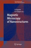
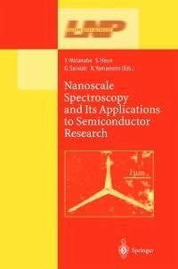
Fabrication technologies for nanostructured devices have be- en developed recently, and the electrical and optical pro- perties of such nanostructures are a subject of advanced re- search. This book describes the different approaches to spectroscopic microscopy, i.e., electron beam probe spec- troscopy, spectroscopic photoelectron microscopy, and scan- ning probe spectroscopy. It will be useful as a compact source of reference for the experienced researcher, taking into account at the same time the needs of postgraduate stu- dents and nonspecialist researchers by using a tutorial ap- proach…mehr

Produktbeschreibung
Fabrication technologies for nanostructured devices have be- en developed recently, and the electrical and optical pro- perties of such nanostructures are a subject of advanced re- search. This book describes the different approaches to spectroscopic microscopy, i.e., electron beam probe spec- troscopy, spectroscopic photoelectron microscopy, and scan- ning probe spectroscopy. It will be useful as a compact source of reference for the experienced researcher, taking into account at the same time the needs of postgraduate stu- dents and nonspecialist researchers by using a tutorial ap- proach throughout. Fabrication technologies for nano-structured devices have been developed recently, and the electrical and optical properties of such nonostructures are a subject of advanced research. This book describes the different approaches to spectroscopic microscopy, that is, Electron Beam Probe Spectroscopy, Spectroscopic Photoelectron Microscopy, and Scanning Probe Spectroscopy. It will be useful as a compact source of reference for the experienced reseracher,taking at the same time into account the needs of post graduate students and nonspecialist researchers by using a tutorial approach throughout.

Dieser Download kann aus rechtlichen Gründen nur mit Rechnungsadresse in A, B, BG, CY, CZ, D, DK, EW, E, FIN, F, GR, HR, H, IRL, I, LT, L, LR, M, NL, PL, P, R, S, SLO, SK ausgeliefert werden.

Autorenporträt
Yoshio Watanabe, NTT Basic Research Laboratories, Kanagawa, Japan / Stefan Heun, Sincrotrone Trieste, Italy / Giancarlo Salviati, Istituto MASPEC, Parma, Italy / Naoki Yamamoto, Tokyo Institute of Technology, Tokyo, Japan
Rezensionen
"This is an unusual collection and the vast audience of workers on semiconductor structure will want to have access to it." (Ultramicroscopy, 99, 2004)