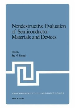
From September 19-29, a NATO Advanced Study Institute on Non destructive Evaluation of Semiconductor Materials and Devices was held at the Villa Tuscolano in Frascati, Italy. A total of 80 attendees and lecturers participated in the program which covered many of the important topics in this field. The subject matter was divided to emphasize the following different types of problems: electrical measurements; acoustic measurements; scanning techniques; optical methods; backscatter methods; x-ray observations; accele rated life tests. It would be difficult to give a full discussion of such an Institute without going through the major points of each speaker. Clearly this is the proper task of the eventual readers of these Proceedings. Instead, it would be preferable to stress some general issues. What came through very clearly is that the measurements of the basic scientists in materials and device phenomena are of sub stantial immediate concern to the device technologies and end users.
Dieser Download kann aus rechtlichen Gründen nur mit Rechnungsadresse in A, B, BG, CY, CZ, D, DK, EW, E, FIN, F, GR, HR, H, IRL, I, LT, L, LR, M, NL, PL, P, R, S, SLO, SK ausgeliefert werden.
Hinweis: Dieser Artikel kann nur an eine deutsche Lieferadresse ausgeliefert werden.

