Alle Infos zum eBook verschenken
- Format: PDF
- Merkliste
- Auf die Merkliste
- Bewerten Bewerten
- Teilen
- Produkt teilen
- Produkterinnerung
- Produkterinnerung
Hier können Sie sich einloggen
Bitte loggen Sie sich zunächst in Ihr Kundenkonto ein oder registrieren Sie sich bei bücher.de, um das eBook-Abo tolino select nutzen zu können.
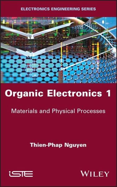
Due to their special properties, organic semiconductors enable the development of large-area, low-cost devices, paving the way for flexible and nomadic applications that advantageously replace those made with traditional semiconductors. This book describes the properties and deposition methods of organic semiconductors, transparent conductive materials or metals which are used in the fabrication of organic devices. The physical processes (optical, electrical and interface) that control the mechanisms in the formation and transport of the charge carriers of the materials are studied and…mehr
- Geräte: PC
- mit Kopierschutz
- eBook Hilfe
- Größe: 3.7MB
- Thien-Phap NguyenOrganic Electronics 2 (eBook, PDF)139,99 €
- Michael C. PettyOrganic and Molecular Electronics (eBook, PDF)71,99 €
- Polymers for Light-emitting Devices and Displays (eBook, PDF)173,99 €
- K. M. GuptaAdvanced Electrical and Electronics Materials (eBook, PDF)153,99 €
- M. Jamal DeenSilicon Photonics (eBook, PDF)150,99 €
- Photoconductivity and Photoconductive Materials (eBook, PDF)300,99 €
- Valeri P. TolstoyHandbook of Infrared Spectroscopy of Ultrathin Films (eBook, PDF)407,99 €
-
-
-
Dieser Download kann aus rechtlichen Gründen nur mit Rechnungsadresse in A, B, BG, CY, CZ, D, DK, EW, E, FIN, F, GR, HR, H, IRL, I, LT, L, LR, M, NL, PL, P, R, S, SLO, SK ausgeliefert werden.
- Produktdetails
- Verlag: John Wiley & Sons
- Seitenzahl: 208
- Erscheinungstermin: 12. März 2021
- Englisch
- ISBN-13: 9781119818922
- Artikelnr.: 61336095
- Verlag: John Wiley & Sons
- Seitenzahl: 208
- Erscheinungstermin: 12. März 2021
- Englisch
- ISBN-13: 9781119818922
- Artikelnr.: 61336095
- Herstellerkennzeichnung Die Herstellerinformationen sind derzeit nicht verfügbar.
Chapter 1. Semiconductor Theory 1
1.1. Introduction 1
1.2. Review of the basic concepts of crystalline semiconductors 3
1.2.1. Intrinsic semiconductors 4
1.2.2. Extrinsic semiconductors 5
1.2.3. Fermi level 7
1.2.4. Charge transport in semiconductors 7
1.3. P-N junction 9
1.3.1. Space charge region 9
1.3.2. Junction capacitance 11
1.4. Impurities and defects 11
1.4.1. Traps and recombination centers 12
1.5. Metal/semiconductor contact 20
1.5.1. Parameters of metal/semiconductor contacts 20
1.5.2. Formation of metal/semiconductor contacts 21
1.5.3. Width ¿ of the space charge region 23
1.5.4. Junction capacitance 23
1.5.5. Schottky effect 24
1.5.6. Schottky diode 25
1.6. Semiconductors under non-equilibrium conditions 27
1.6.1. Parameters of a semiconductor under non-equilibrium conditions 27
1.6.2. Recombination of carriers via recombination centers
(Shockley-Read-Hall theory) 29
1.6.3. Transient relaxation current 31
1.7. Space charge current 34
1.7.1. The case of an ideal semiconductor 35
1.7.2. Trap-filled limit voltage 37
1.7.3. Discrete traps and trap distribution 37
1.8. Hopping conduction 38
Chapter 2. Materials 41
2.1. Introduction 41
2.2. Organic materials 42
2.2.1. Binding and hybridization of carbon 46
2.3. Conjugated polymers 48
2.3.1. Polyacetylene 49
2.3.2. Benzene 51
2.3.3. Deposition of polymer films 52
2.4. Energy bands 53
2.4.1. Concepts of solitons and polarons 55
2.4.2. Concept of doping 58
2.5. Small molecules 61
2.6. Design and engineering of organic materials 63
2.7. Hybrid materials or nanocomposites 65
2.7.1. Polymer matrix nanocomposites 67
2.7.2. Nanocomposites with nanomaterials 67
2.7.3. Preparation of nanocomposites 68
2.8. Transparent and conductive materials 73
2.8.1. Indium tin oxide 73
2.8.2. Fluorine-doped tin oxide 74
2.8.3. Other transparent oxide conductors 75
2.8.4. Other transparent conductive materials 75
2.9. Materials for encapsulation 78
2.9.1. Glass slides 78
2.9.2. Hybrid multilayers 79
Chapter 3. Optical Processes 81
3.1. Introduction 81
3.2. Interaction between light and molecules 81
3.2.1. Electronic transitions 81
3.2.2. Selection rules 82
3.3. Optical processes 84
3.3.1. Light absorption 84
3.3.2. Light emission 88
3.3.3. Perrin-Jablonski diagram 91
3.3.4. Quenching 91
3.4. Excitons 99
3.4.1. Classification of excitons 100
3.4.2. Binding energy of excitons 101
3.4.3. Movement of excitons 103
3.4.4. Dissociation of excitons 103
3.5. Experimental techniques 104
3.5.1. UV-visible absorption spectroscopy 104
3.5.2. Photoluminescence spectroscopy 106
3.5.3. Infrared and Raman spectroscopy 110
Chapter 4. Electronic Processes 115
4.1. Introduction 115
4.2. Charge carrier injection process 116
4.2.1. Injection mechanisms 117
4.2.2. Hole or electron devices 119
4.2.3. Transport layers 121
4.3. Charge transport process 123
4.3.1. Hopping mechanisms 124
4.3.2. Space-charge limited conduction 133
4.3.3. Defects and traps in organic semiconductors 140
Chapter 5. Interface Processes 155
5.1. Introduction 155
5.2. Formation of organic semiconductor/metal interfaces 155
5.2.1. Vacuum-level alignment model: Mott-Schottky theory 156
5.2.2. Interface dipole model: Bardeen's theory 156
5.2.3. Characteristics of organic semiconductor/metal interfaces 158
5.2.4. Fermi-level pinning 160
5.2.5. Integer charge transfer process 162
5.3. Surface characterization techniques 166
5.3.1. Atomic force microscopy 166
5.3.2. X-ray photoelectron spectroscopy 167
5.3.3. UV photoelectron spectroscopy 168
5.4. Interface engineering 169
5.4.1. Inverted structure devices 170
5.4.2. Self-assembled monolayers 172
5.5. Conclusion 174
List of Acronyms 175
References 183
Index 191