Lech Pawlowski
Physical Deposition Methods for Films and Coatings (eBook, PDF)
159,99 €
159,99 €
inkl. MwSt.
Sofort per Download lieferbar
0 °P sammeln
159,99 €
Als Download kaufen
159,99 €
inkl. MwSt.
Sofort per Download lieferbar
0 °P sammeln
Jetzt verschenken
Alle Infos zum eBook verschenken
159,99 €
inkl. MwSt.
Sofort per Download lieferbar
Alle Infos zum eBook verschenken
0 °P sammeln
Lech Pawlowski
Physical Deposition Methods for Films and Coatings (eBook, PDF)
- Format: PDF
- Merkliste
- Auf die Merkliste
- Bewerten Bewerten
- Teilen
- Produkt teilen
- Produkterinnerung
- Produkterinnerung
Bitte loggen Sie sich zunächst in Ihr Kundenkonto ein oder registrieren Sie sich bei
bücher.de, um das eBook-Abo tolino select nutzen zu können.
Hier können Sie sich einloggen
Sie sind bereits eingeloggt. Klicken Sie auf 2. tolino select Abo, um fortzufahren.
Bitte loggen Sie sich zunächst in Ihr Kundenkonto ein oder registrieren Sie sich bei bücher.de, um das eBook-Abo tolino select nutzen zu können.
Comprehensive resource on the subject of deposition techniques for films and coatings and their characterization
Physical Deposition Methods for Films and Coatings presents a pedagogical compilation of current knowledge of dry deposition.
Written by a renowned and awarded academic with more than 40 years of experience in the field, Physical Deposition Methods for Films and Coatings covers topics including:
The process of making a deposit that appears on the surface, growth of deposits, their post treatments, and characterization methods | Different physical and chemical deposition…mehr
- Geräte: PC
- mit Kopierschutz
- eBook Hilfe
- Größe: 14.55MB
Andere Kunden interessierten sich auch für
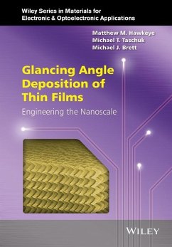
- Matthew M. HawkeyeGlancing Angle Deposition of Thin Films (eBook, PDF)114,99 €
- Pulsed Laser Deposition of Thin Films (eBook, PDF)217,99 €
- Atomic Layer Deposition in Energy Conversion Applications (eBook, PDF)142,99 €
- Atomic Layer Deposition of Nanostructured Materials (eBook, PDF)156,99 €
- Organized Organic Ultrathin Films (eBook, PDF)111,99 €
- Novel Anti-Corrosion and Anti-Fouling Coatings and Thin Films (eBook, PDF)194,99 €
- Integration of Ferroelectric and Piezoelectric Thin Films (eBook, PDF)201,99 €
-
-
-
Comprehensive resource on the subject of deposition techniques for films and coatings and their characterization
Physical Deposition Methods for Films and Coatings presents a pedagogical compilation of current knowledge of dry deposition.
Written by a renowned and awarded academic with more than 40 years of experience in the field, Physical Deposition Methods for Films and Coatings covers topics including:
Physical Deposition Methods for Films and Coatings is an essential reference on the subject for professionals and researchers in surface treatment and graduate students in related programs of study.
Physical Deposition Methods for Films and Coatings presents a pedagogical compilation of current knowledge of dry deposition.
Written by a renowned and awarded academic with more than 40 years of experience in the field, Physical Deposition Methods for Films and Coatings covers topics including:
- The process of making a deposit that appears on the surface, growth of deposits, their post treatments, and characterization methods
- Different physical and chemical deposition techniques including atomistic, chemical vapor, and various thermal spraying methods
- Properties of deposits depending on the material and deposition technique
- Substrate preparation, coating microstructure, and morphology and stability of thin films
- Examples of applications of thin films in optical devices, environmental applications, telecommunications devices, and energy storage devices
Physical Deposition Methods for Films and Coatings is an essential reference on the subject for professionals and researchers in surface treatment and graduate students in related programs of study.
Dieser Download kann aus rechtlichen Gründen nur mit Rechnungsadresse in D ausgeliefert werden.
Produktdetails
- Produktdetails
- Verlag: Wiley
- Seitenzahl: 431
- Erscheinungstermin: 14. Januar 2025
- Englisch
- ISBN-13: 9781119713111
- Artikelnr.: 72863461
- Verlag: Wiley
- Seitenzahl: 431
- Erscheinungstermin: 14. Januar 2025
- Englisch
- ISBN-13: 9781119713111
- Artikelnr.: 72863461
- Herstellerkennzeichnung Die Herstellerinformationen sind derzeit nicht verfügbar.
Lech Pawlowski is a professor emeritus at the University of Limoges in France. He has more than 40 years of experience working with and researching coatings of different materials. He was honored by doctorate honoris causa attributed by Chemnitz University of Technology in Germany and through introduction into the Hall of Fame of Thermal Spray Society by the American Society of Materials. He has authored and co-authored over 100 papers.
Preface xiii
Abbreviations and Symbols xv
Introduction xxv
1 Substrate Preparation 1
1.1 Introduction 1
1.2 Surfaces of Different Types of Substrates (Metals and Alloys, Ceramics,
Polymers) 2
1.2.1 Metals and Alloys 4
1.2.2 Ceramics and Glasses 8
1.2.3 Polymers 11
1.3 Cleaning of Surface 14
1.3.1 Chemical Cleaning Methods 14
1.3.2 Physical Cleaning Methods 16
1.3.2.1 Thermal Cleaning 16
1.3.2.2 Particles Cleaning 17
1.3.2.3 Plasma Cleaning 17
1.3.2.4 Ions and Atoms Bombardment 20
1.3.2.5 Ultrasonic Cleaning 22
1.3.2.6 Photons Cleaning 22
1.3.3 Monitoring of Surface 24
1.4 Patterning of Films and Coatings 25
1.4.1 Lithography 27
1.4.1.1 Illumination 28
1.4.1.2 Masks 29
1.4.1.3 Geometry of Lithography 30
1.4.1.4 Etching and Removal Processes 30
1.4.2 Direct Patterning 31
1.4.2.1 Photons Patterning 31
1.4.2.2 Particles Patterning 32
1.5 Activation of Substrates Surface 32
1.5.1 Activation of Substrates at Atomistic Deposition 33
1.5.1.1 Liquids Activation 34
1.5.1.2 Photons Activation 34
1.5.1.3 Particles Activation 34
1.5.2 Activation of the Substrates Before Granular Deposits 38
1.5.2.1 Particles Activation 38
1.5.2.2 Photons Activation 39
1.5.2.3 Water jet Activation 40
1.5.2.4 Plasma Activation 40
References 42
2 Films and Coatings Deposition Techniques 49
2.1 Introduction 49
2.2 Atomistic Deposition Methods 49
2.2.1 Physical Vapor Deposition (PVD) by Thermal Evaporation 50
2.2.1.1 History 50
2.2.1.2 Principle 51
2.2.1.3 Sources 52
2.2.1.4 Medium 55
2.2.2 Physical Vapor Deposition (PVD) by Sputtering 57
2.2.2.1 History 57
2.2.2.2 Principle 58
2.2.2.3 Source 59
2.2.2.4 Medium 62
2.2.3 Ion plating and i-beam-assisted Deposition 63
2.2.3.1 History 63
2.2.3.2 Principle 63
2.2.4 Pulsed-Laser Deposition (PLD) 65
2.2.4.1 History 65
2.2.4.2 Principle 66
2.2.4.3 Source 68
2.2.4.4 Medium 68
2.2.5 Chemical Vapor Deposition (CVD) 69
2.2.5.1 History 70
2.2.5.2 Principle and Techniques 70
2.2.5.3 Sources in CVD Techniques 71
2.2.5.4 Thermal CVD 71
2.2.5.5 Pe Cvd 77
2.2.5.6 Laser-Assisted Chemical Vapor Deposition (LCVD) 80
2.2.5.7 Metal-Organic Chemical Vapor Deposition (MO CVD) 83
2.2.5.8 Atomic Layer Deposition (ALD) 84
2.3 Granular Methods of Coatings Deposition 85
2.3.1 Powder Fedstock 85
2.3.1.1 Methods of Powder Manufacturing 86
2.3.1.2 Characterization of Powders 90
2.3.1.3 Delivery and Injection of Powder to Flame and Plasma 90
2.3.2 Solid Feedstock Deposition Methods 91
2.3.2.1 Flame Spraying (FS) 92
2.3.2.2 Arc Spraying (AS) 93
2.3.2.3 Atmospheric Plasma Spraying (APS) 94
2.3.2.4 High-Velocity Oxy-Fuel Spraying (HVOF) 98
2.3.2.5 Detonation Spraying 101
2.3.2.6 Cold Gas Spraying Method (CGSM) 102
2.3.2.7 Vacuum Plasma Spraying (VPS) 104
2.3.2.8 Plasma Spray Physical Vapor Deposition (PS PVD) 105
2.3.3 Liquid Feedstock Deposition Method 107
2.3.3.1 Solutions Preparation 108
2.3.3.2 Suspension Preparation 108
2.3.3.3 Delivery and Injection of Liquid to Flame or Plasma 110
2.3.3.4 Spray Pyrolysis (SP) 111
2.3.3.5 Suspension Plasma Spraying (SPS) 112
2.3.3.6 Solution Precursor Plasma Spraying (SPPS) 114
2.4 Bulk Methods of Coatings Deposition 115
2.4.1 Plasma Transferred Arc (PTA) 116
2.4.2 Laser Coatings 117
2.4.2.1 1-Step Laser Deposition (1SLD) 118
2.4.2.2 2-step Laser Deposition (2SLD) 121
References 125
3 Nucleation, Growth, and Microstructure of Physical Deposits 137
3.1 Introduction 137
3.2 Atomistic Deposition Methods 138
3.2.1 Introduction 138
3.2.2 Phenomena at Contact and Nucleation 138
3.2.2.1 Growth in Three Dimensions 140
3.2.2.2 Nucleation and Growth in Two Dimensions 141
3.2.2.3 Nucleation and Growth in Two Dimensions and in Three Dimensions 142
3.2.3 Interface Between Film and Substrate 142
3.2.4 Microstructure of Films Obtained Using Different Deposition
Techniques 143
3.2.5 Residual Stresses and Defects in Films 147
3.2.6 Post-deposition Treatment 149
3.3 Granular Deposits 150
3.3.1 Introduction 150
3.3.2 Contact Phenomena 151
3.3.2.1 Deformation of a Particle 151
3.3.2.2 Solidification and Cooling of a Particle 154
3.3.2.3 Adhesion Mechanisms 155
3.3.3 Nucleation and Growth of a Crystal 157
3.3.3.1 Phase Composition 158
3.3.3.2 Inhomogeneity of Deposits, Composites 160
3.3.4 Build-up of a Coating 162
3.3.4.1 Temperature of a Coating 163
3.3.4.2 Residual Stresses 165
3.3.5 Post-deposition Treatment 167
3.4 Bulk Deposits 168
3.4.1 Introduction 168
3.4.2 Phenomena in the Melt-pool 170
3.4.3 Laser Shock Treatment 172
3.4.4 Nucleation in the Melt Pool 172
3.4.5 Inhomogeneities of Deposits and Thermal Stresses 176
3.4.6 Post-deposit Treatment 176
References 177
4 Methods of Films and Coatings Characterization 185
4.1 Introduction 185
4.2 Methods of Microstructure Characterization 186
4.2.1 Chemical Composition Analyses 187
4.2.1.1 Auger Electron Spectroscopy (AES) 187
4.2.1.2 Energy-dispersive X-ray Spectroscopy (EDX) 190
4.2.1.3 Wavelength-dispersive X-ray Spectroscopy (WDX) 191
4.2.1.4 Electron Energy Loss Spectroscopy (EELS) 192
4.2.1.5 Electron Microprobe Analysis (EMPA) 193
4.2.1.6 Raman Spectroscopy (RS) 194
4.2.1.7 X-ray Photoelectron Spectroscopy (XPS) 195
4.2.1.8 X-ray Fluorescence Spectroscopy 197
4.2.2 Crystallographic Analyses 198
4.2.2.1 X-ray Diffraction (XRD) 198
4.2.2.2 Selected Area Diffraction (SAD) 199
4.2.2.3 Electron Backscatter Diffraction (EBSD) 200
4.2.3 Analyses of Morphology 201
4.2.3.1 Optical Microscope (OM) 201
4.2.3.2 Scanning Electron Microscope (SEM) 202
4.2.3.3 Scanning Tunneling Microscope (STM) 203
4.2.3.4 Atomic Force Microscope (AFM) 205
4.2.3.5 Transmission Electron Microscope (TEM) 205
4.3 Mechanical Properties of Films and Coatings 208
4.3.1 Fundamentals of Mechanical Properties 208
4.3.2 Adhesion 210
4.3.3 Hardness and Microhardness 211
4.3.4 Elasticity of Deposits 213
4.3.5 Fracture Toughness 215
4.3.6 Friction and Wear 216
4.3.7 Residual Stresses 219
4.4 Physical Properties of Films and Coatings 220
4.4.1 Thickness 220
4.4.2 Porosity 220
4.4.3 Thermophysical Properties 222
4.4.3.1 Thermal Conductivity 223
4.4.3.2 Specific Heat and Thermal Expansion 224
4.4.3.3 Emissivity 225
4.4.3.4 Thermal Shock Resistance 225
4.4.4 Contact Angle 225
4.5 Corrosion Resistance 226
4.5.1 Aqueous Corrosion 226
4.5.2 Hot Corrosion 229
4.6 Electric and Magnetic Properties of Films and Coatings 229
4.6.1 Electric Conductivity and Resistivity 230
4.6.2 Dielectric Properties 232
4.6.3 Magnetic Properties 234
4.7 Optical Properties of Films and Coatings 235
4.8 Characterization of Biomaterials 238
4.8.1 Introduction 238
4.8.2 In vitro Characterization 239
4.8.3 In vivo Characterization 239
References 240
5 Properties of Films and Coatings 251
5.1 Introduction 251
5.2 Mechanical Properties 252
5.2.1 Hardness and Microhardness 252
5.2.1.1 Atomistic Films 252
5.2.1.2 Granular Coatings 257
5.2.1.3 Bulk Deposits 263
5.2.2 Adhesion 265
5.2.2.1 Atomistic Deposits 269
5.2.2.2 Granular Deposits 272
5.2.3 Elasticity, Strength, and Toughness 274
5.2.3.1 Atomistic Deposits 274
5.2.3.2 Granular Deposits 275
5.2.4 Friction and Wear 283
5.2.4.1 Atomistic Deposits 284
5.2.4.2 Granular Coatings 287
5.2.4.3 Bulk Coatings 297
5.2.5 Example of Coatings Applications: Anilox Rolls 302
5.3 Electric and Magnetic Properties 304
5.3.1 Conductors and Resistors 304
5.3.1.1 Atomistic Deposits 305
5.3.1.2 Granular Deposits 307
5.3.2 Dielectric Properties 309
5.3.2.1 Atomistic Deposits 310
5.3.2.2 Granular Deposits 310
5.3.3 Magnetic Properties 313
5.3.3.1 Atomistic Deposits 313
5.3.3.2 Granular Deposits 315
5.3.4 Superconductors 315
5.3.4.1 Atomistic Deposits 317
5.3.4.2 Granular Deposits 317
5.3.5 Electron Emitters 317
5.3.5.1 Atomistic Films 319
5.3.5.2 Granular Coatings 319
5.4 Thermophysical Properties 321
5.4.1 Thermal Conductivity and Diffusivity 322
5.4.1.1 Atomistic Deposits 322
5.4.1.2 Granular Deposits 323
5.4.2 Emissivity 328
5.5 Corrosion Resistance 332
5.5.1 Aqueous Corrosion 332
5.5.1.1 Atomistic Films 334
5.5.1.2 Granular Coatings 334
5.5.1.3 Bulk Deposits 336
5.5.2 Hot Corrosion 338
5.5.2.1 Atomistic Deposits 342
5.5.2.2 Granular Deposits 342
5.5.2.3 Bulk Deposits 345
5.6 Optical Properties 345
5.6.1 Decorative Deposits 345
5.6.2 Functional Deposits 349
5.7 Biomaterials 349
5.7.1 Atomistic Deposits 351
5.7.2 Granular Deposits 353
References 357
Index 381