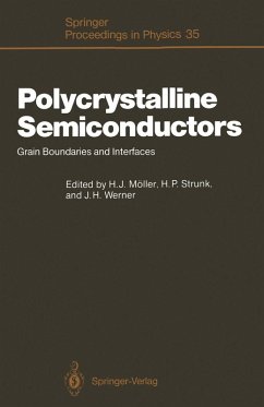
Polycrystalline Semiconductors (eBook, PDF)
Grain Boundaries and Interfaces
Redaktion: Möller, Hans J.; Werner, Jürgen H.; Strunk, Horst P.
113,95 €
113,95 €
inkl. MwSt.
Sofort per Download lieferbar

57 °P sammeln
113,95 €
Als Download kaufen

113,95 €
inkl. MwSt.
Sofort per Download lieferbar

57 °P sammeln
Jetzt verschenken
Alle Infos zum eBook verschenken
113,95 €
inkl. MwSt.
Sofort per Download lieferbar
Alle Infos zum eBook verschenken

57 °P sammeln
Polycrystalline Semiconductors (eBook, PDF)
Grain Boundaries and Interfaces
Redaktion: Möller, Hans J.; Werner, Jürgen H.; Strunk, Horst P.
- Format: PDF
- Merkliste
- Auf die Merkliste
- Bewerten Bewerten
- Teilen
- Produkt teilen
- Produkterinnerung
- Produkterinnerung

Bitte loggen Sie sich zunächst in Ihr Kundenkonto ein oder registrieren Sie sich bei
bücher.de, um das eBook-Abo tolino select nutzen zu können.
Hier können Sie sich einloggen
Hier können Sie sich einloggen
Sie sind bereits eingeloggt. Klicken Sie auf 2. tolino select Abo, um fortzufahren.

Bitte loggen Sie sich zunächst in Ihr Kundenkonto ein oder registrieren Sie sich bei bücher.de, um das eBook-Abo tolino select nutzen zu können.
- Geräte: PC
- ohne Kopierschutz
- eBook Hilfe
- Größe: 57.07MB
Andere Kunden interessierten sich auch für
![Fundamental Aspects of Silicon Oxidation (eBook, PDF) Fundamental Aspects of Silicon Oxidation (eBook, PDF)]() Fundamental Aspects of Silicon Oxidation (eBook, PDF)73,95 €
Fundamental Aspects of Silicon Oxidation (eBook, PDF)73,95 €![Nanoscale Phenomena in Ferroelectric Thin Films (eBook, PDF) Nanoscale Phenomena in Ferroelectric Thin Films (eBook, PDF)]() Nanoscale Phenomena in Ferroelectric Thin Films (eBook, PDF)161,95 €
Nanoscale Phenomena in Ferroelectric Thin Films (eBook, PDF)161,95 €![Thin-Film Solar Cells (eBook, PDF) Thin-Film Solar Cells (eBook, PDF)]() Thin-Film Solar Cells (eBook, PDF)73,95 €
Thin-Film Solar Cells (eBook, PDF)73,95 €![Silicon Carbide (eBook, PDF) Silicon Carbide (eBook, PDF)]() Silicon Carbide (eBook, PDF)233,95 €
Silicon Carbide (eBook, PDF)233,95 €![Crystal Growth of Silicon for Solar Cells (eBook, PDF) Crystal Growth of Silicon for Solar Cells (eBook, PDF)]() Crystal Growth of Silicon for Solar Cells (eBook, PDF)113,95 €
Crystal Growth of Silicon for Solar Cells (eBook, PDF)113,95 €![Molecular Beam Epitaxy (eBook, PDF) Molecular Beam Epitaxy (eBook, PDF)]() Marian A. HermanMolecular Beam Epitaxy (eBook, PDF)40,95 €
Marian A. HermanMolecular Beam Epitaxy (eBook, PDF)40,95 €![Dilute III-V Nitride Semiconductors and Material Systems (eBook, PDF) Dilute III-V Nitride Semiconductors and Material Systems (eBook, PDF)]() Dilute III-V Nitride Semiconductors and Material Systems (eBook, PDF)113,95 €
Dilute III-V Nitride Semiconductors and Material Systems (eBook, PDF)113,95 €-
-
- -34%11
Produktdetails
- Verlag: Springer Berlin Heidelberg
- Seitenzahl: 394
- Erscheinungstermin: 6. Dezember 2012
- Englisch
- ISBN-13: 9783642934131
- Artikelnr.: 53105123
Dieser Download kann aus rechtlichen Gründen nur mit Rechnungsadresse in A, B, BG, CY, CZ, D, DK, EW, E, FIN, F, GR, HR, H, IRL, I, LT, L, LR, M, NL, PL, P, R, S, SLO, SK ausgeliefert werden.
- Herstellerkennzeichnung Die Herstellerinformationen sind derzeit nicht verfügbar.
I Grain Boundary Structure.- Intergranular Total Energy Maps and the Structure of a Grain Boundary.- Grain Boundary Structure Determination by HREM: A Comparison with Computer Relaxed Configurations for Pure Tilt in Germanium.- Multiple Structures of a [001] ? = 13 Tilt Grain Boundary in Germanium.- Computer Modelling of Grain Boundaries by Use of Interatomic Potentials.- Transmission of Dislocations with Non-common Burgers Vectors Through ? = 9 (12?2) Boundaries in Silicon and Germanium Observed by In Situ HVEM.- II Grain Boundary Chemistry and Electronic Properties.- High Resolution Electron Microscopy of the Structure and Chemistry of Grain Boundaries and Other Interfaces in Semiconductors.- Theoretical Studies of the Impurity Segregation and Electrical Properties of Polycrystalline Silicon by LCAO Electronic Theory.- Electronic Properties of ? = 25 Silicon Bicrystals by Deep Level Transient Spectroscopy.- The Influence of Structure and Impurity Precipitation on the Electrical Properties of the Grain Boundaries in Silicon: Copper Precipitation in the ? = 25 Boundary.- EBIC Contrast and Precipitation in ? = 13 and ? = 25 Annealed Silicon Bicrystals.- Electron Beam Induced Current Contrast and Transmission Electron Microscopy Analysis of Special Grain Boundaries in Silicon.- SEM-EBIC Investigations of the Electrical Activity of Grain Boundaries in Germanium.- III Segregation, Activation and Passivation.- Atomic-Level Imaging and Microanalysis of Grain Boundaries in Polycrystalline Semiconductors.- Investigation of the Cobalt Segregation at Grain Boundaries in Silicon.- On the Influence of the Cottrell Atmosphere on the Recombination Losses at Grain Boundaries in Polycrystalline Silicon.- Hydrogen Passivation of Grain Boundaries in Silicon Sheet Material.-Atomic Hydrogen Passivation Studies of Microcrystalline Phases in Ion-Implant Damaged Surface Layers of Silicon.- Hydrogen Injection and Migration in Silicon.- Analysis of the Polycrystalline Semiconducting Film Electrical Resistance Variation Due to Isothermal Desorption and Temperature Stimulated Desorption of Oxygen.- IV Segregation, Activation and Passivation.- Activation and Passivation of Grain Boundary Recombination Activity in Polycrystalline Silicon.- Thermal Activation and Hydrogen Passivation of Grain Boundaries.- Analysis of Metal-Doped Polycrystalline Silicon with Secondary Ion Mass Spectrometry.- Oxygen Detection in Polycrystalline Silicon.- Generation of Radiation Defects in the Vicinity of Twin Boundaries in EFG Silicon Ribbons.- Physical Properties of Polycrystalline S-Web Si Ribbons.- Grain Boundary Structure in S-WEB Silicon Ribbon.- Characterization of MBE-Grown Polysilicon.- V Technology.- Mechanisms of Epitaxial Growth of Polar Semiconductors on (001) Silicon.- Preparation and Characterization of Nickel Silicide.- Characterization of the Interface of Silicon pn-Junctions, Fabricated by the Silicon Direct Bonding (SDB) Method.- Metal and Polycrystalline Silicon Reactions.- Interfacial Reactions of TiNx/Si Contacts.- Linear and Parabolic Growth Kinetics in Binary Couples.- VI Thin Films.- Polycrystalline Compound Semiconductor Thin Films in Solar Cells.- Electronic Properties of Photoetched CdSe Films.- Thin Film Transistors and Light Sensors with Polycrystalline CdSe-Semiconductors.- VII Crystallization.- Crystallization Processes and Structures of Semiconductor Films.- Crystallized Silicon Films for Active Devices.- Laser Recrystallization of Polysilicon for Improved Device Quality.- Growth of Sb-Doped Epitaxial Si Layers Through Recrystallizationof Poly-Si on a (100) Si Substrate.- VIII Transport Properties.- Current Control by Electrically Active Grain Boundaries.- Numerical Modelling of the Intergranular Potential Barrier Height and Carrier Concentration in Polysilicon.- Hall Mobility and Carrier Concentration of e-Gun Evaporated Poly-Si Films.- Measurement and Calculation of the Carrier Concentration in Polycrystalline Germanium Thin Films.- Grain Boundary States in Float-Zone Silicon Bicrystals.- Pressure Studies of Metastable Electron Traps in Grain Boundaries of p-HgMnTe and p-HgCdMnTe.- Band Tailing in Polycrystalline and Disordered Silicon.- IX Thin Films.- Microstructure and Interfaces of Polysilicon in Integrated Circuits.- Effect of the Grain Boundaries in Small Grain Polysilicon Thin Film Transistors.- Kink Effect in the Double-Gate Accumulation-Mode N-Channel Polysilicon Thin-Film Transistors.- Applications of Poly-Si in Selective-Area and Three-Dimensional Devices.- Thin-Film Transistors from Evaporated Low Temperature Processed Poly-Si Films.- Pressure Effect on In Situ Boron-Doped LPCVD Silicon Films.- Index of Contributors.
I Grain Boundary Structure.- Intergranular Total Energy Maps and the Structure of a Grain Boundary.- Grain Boundary Structure Determination by HREM: A Comparison with Computer Relaxed Configurations for Pure Tilt in Germanium.- Multiple Structures of a [001] ? = 13 Tilt Grain Boundary in Germanium.- Computer Modelling of Grain Boundaries by Use of Interatomic Potentials.- Transmission of Dislocations with Non-common Burgers Vectors Through ? = 9 (12?2) Boundaries in Silicon and Germanium Observed by In Situ HVEM.- II Grain Boundary Chemistry and Electronic Properties.- High Resolution Electron Microscopy of the Structure and Chemistry of Grain Boundaries and Other Interfaces in Semiconductors.- Theoretical Studies of the Impurity Segregation and Electrical Properties of Polycrystalline Silicon by LCAO Electronic Theory.- Electronic Properties of ? = 25 Silicon Bicrystals by Deep Level Transient Spectroscopy.- The Influence of Structure and Impurity Precipitation on the Electrical Properties of the Grain Boundaries in Silicon: Copper Precipitation in the ? = 25 Boundary.- EBIC Contrast and Precipitation in ? = 13 and ? = 25 Annealed Silicon Bicrystals.- Electron Beam Induced Current Contrast and Transmission Electron Microscopy Analysis of Special Grain Boundaries in Silicon.- SEM-EBIC Investigations of the Electrical Activity of Grain Boundaries in Germanium.- III Segregation, Activation and Passivation.- Atomic-Level Imaging and Microanalysis of Grain Boundaries in Polycrystalline Semiconductors.- Investigation of the Cobalt Segregation at Grain Boundaries in Silicon.- On the Influence of the Cottrell Atmosphere on the Recombination Losses at Grain Boundaries in Polycrystalline Silicon.- Hydrogen Passivation of Grain Boundaries in Silicon Sheet Material.-Atomic Hydrogen Passivation Studies of Microcrystalline Phases in Ion-Implant Damaged Surface Layers of Silicon.- Hydrogen Injection and Migration in Silicon.- Analysis of the Polycrystalline Semiconducting Film Electrical Resistance Variation Due to Isothermal Desorption and Temperature Stimulated Desorption of Oxygen.- IV Segregation, Activation and Passivation.- Activation and Passivation of Grain Boundary Recombination Activity in Polycrystalline Silicon.- Thermal Activation and Hydrogen Passivation of Grain Boundaries.- Analysis of Metal-Doped Polycrystalline Silicon with Secondary Ion Mass Spectrometry.- Oxygen Detection in Polycrystalline Silicon.- Generation of Radiation Defects in the Vicinity of Twin Boundaries in EFG Silicon Ribbons.- Physical Properties of Polycrystalline S-Web Si Ribbons.- Grain Boundary Structure in S-WEB Silicon Ribbon.- Characterization of MBE-Grown Polysilicon.- V Technology.- Mechanisms of Epitaxial Growth of Polar Semiconductors on (001) Silicon.- Preparation and Characterization of Nickel Silicide.- Characterization of the Interface of Silicon pn-Junctions, Fabricated by the Silicon Direct Bonding (SDB) Method.- Metal and Polycrystalline Silicon Reactions.- Interfacial Reactions of TiNx/Si Contacts.- Linear and Parabolic Growth Kinetics in Binary Couples.- VI Thin Films.- Polycrystalline Compound Semiconductor Thin Films in Solar Cells.- Electronic Properties of Photoetched CdSe Films.- Thin Film Transistors and Light Sensors with Polycrystalline CdSe-Semiconductors.- VII Crystallization.- Crystallization Processes and Structures of Semiconductor Films.- Crystallized Silicon Films for Active Devices.- Laser Recrystallization of Polysilicon for Improved Device Quality.- Growth of Sb-Doped Epitaxial Si Layers Through Recrystallizationof Poly-Si on a (100) Si Substrate.- VIII Transport Properties.- Current Control by Electrically Active Grain Boundaries.- Numerical Modelling of the Intergranular Potential Barrier Height and Carrier Concentration in Polysilicon.- Hall Mobility and Carrier Concentration of e-Gun Evaporated Poly-Si Films.- Measurement and Calculation of the Carrier Concentration in Polycrystalline Germanium Thin Films.- Grain Boundary States in Float-Zone Silicon Bicrystals.- Pressure Studies of Metastable Electron Traps in Grain Boundaries of p-HgMnTe and p-HgCdMnTe.- Band Tailing in Polycrystalline and Disordered Silicon.- IX Thin Films.- Microstructure and Interfaces of Polysilicon in Integrated Circuits.- Effect of the Grain Boundaries in Small Grain Polysilicon Thin Film Transistors.- Kink Effect in the Double-Gate Accumulation-Mode N-Channel Polysilicon Thin-Film Transistors.- Applications of Poly-Si in Selective-Area and Three-Dimensional Devices.- Thin-Film Transistors from Evaporated Low Temperature Processed Poly-Si Films.- Pressure Effect on In Situ Boron-Doped LPCVD Silicon Films.- Index of Contributors.
