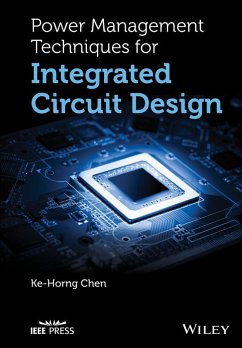
Power Management Techniques for Integrated Circuit Design (eBook, PDF)


Alle Infos zum eBook verschenken

Power Management Techniques for Integrated Circuit Design (eBook, PDF)
- Format: PDF
- Merkliste
- Auf die Merkliste
- Bewerten Bewerten
- Teilen
- Produkt teilen
- Produkterinnerung
- Produkterinnerung

Hier können Sie sich einloggen

Bitte loggen Sie sich zunächst in Ihr Kundenkonto ein oder registrieren Sie sich bei bücher.de, um das eBook-Abo tolino select nutzen zu können.
This book begins with the premise that energy demands are directing scientists towards ever-greener methods of power management, so highly integrated power control ICs (integrated chip/circuit) are increasingly in demand for further reducing power consumption. * A timely and comprehensive reference guide for IC designers dealing with the increasingly widespread demand for integrated low power management * Includes new topics such as LED lighting, fast transient response, DVS-tracking and design with advanced technology nodes * Leading author (Chen) is an active and renowned contributor to the…mehr
- Geräte: PC
- mit Kopierschutz
- eBook Hilfe
- Größe: 42.35MB
![Statistical Analysis and Optimization for VLSI: Timing and Power (eBook, PDF) Statistical Analysis and Optimization for VLSI: Timing and Power (eBook, PDF)]() Ashish SrivastavaStatistical Analysis and Optimization for VLSI: Timing and Power (eBook, PDF)113,95 €
Ashish SrivastavaStatistical Analysis and Optimization for VLSI: Timing and Power (eBook, PDF)113,95 €![Timing Optimization Through Clock Skew Scheduling (eBook, PDF) Timing Optimization Through Clock Skew Scheduling (eBook, PDF)]() Ivan S. KourtevTiming Optimization Through Clock Skew Scheduling (eBook, PDF)73,95 €
Ivan S. KourtevTiming Optimization Through Clock Skew Scheduling (eBook, PDF)73,95 €![Practical Problems in VLSI Physical Design Automation (eBook, PDF) Practical Problems in VLSI Physical Design Automation (eBook, PDF)]() Sung Kyu LimPractical Problems in VLSI Physical Design Automation (eBook, PDF)113,95 €
Sung Kyu LimPractical Problems in VLSI Physical Design Automation (eBook, PDF)113,95 €![Digital VLSI Design and Simulation with Verilog (eBook, PDF) Digital VLSI Design and Simulation with Verilog (eBook, PDF)]() Suman Lata TripathiDigital VLSI Design and Simulation with Verilog (eBook, PDF)106,99 €
Suman Lata TripathiDigital VLSI Design and Simulation with Verilog (eBook, PDF)106,99 €![Green Communication with Field-programmable Gate Array for Sustainable Development (eBook, PDF) Green Communication with Field-programmable Gate Array for Sustainable Development (eBook, PDF)]() Bishwajeet PandeyGreen Communication with Field-programmable Gate Array for Sustainable Development (eBook, PDF)52,95 €
Bishwajeet PandeyGreen Communication with Field-programmable Gate Array for Sustainable Development (eBook, PDF)52,95 €![Design of Integrated Circuits for Optical Communications (eBook, PDF) Design of Integrated Circuits for Optical Communications (eBook, PDF)]() Behzad RazaviDesign of Integrated Circuits for Optical Communications (eBook, PDF)119,99 €
Behzad RazaviDesign of Integrated Circuits for Optical Communications (eBook, PDF)119,99 €![Fundamentals of Power Integrity for Computer Platforms and Systems (eBook, PDF) Fundamentals of Power Integrity for Computer Platforms and Systems (eBook, PDF)]() Joseph T. DibeneFundamentals of Power Integrity for Computer Platforms and Systems (eBook, PDF)117,99 €
Joseph T. DibeneFundamentals of Power Integrity for Computer Platforms and Systems (eBook, PDF)117,99 €-
-
-
Dieser Download kann aus rechtlichen Gründen nur mit Rechnungsadresse in A, B, BG, CY, CZ, D, DK, EW, E, FIN, F, GR, HR, H, IRL, I, LT, L, LR, M, NL, PL, P, R, S, SLO, SK ausgeliefert werden.
- Produktdetails
- Verlag: John Wiley & Sons
- Seitenzahl: 560
- Erscheinungstermin: 9. Mai 2016
- Englisch
- ISBN-13: 9781118896822
- Artikelnr.: 45055683
- Verlag: John Wiley & Sons
- Seitenzahl: 560
- Erscheinungstermin: 9. Mai 2016
- Englisch
- ISBN-13: 9781118896822
- Artikelnr.: 45055683
- Herstellerkennzeichnung Die Herstellerinformationen sind derzeit nicht verfügbar.
Preface xiii
Acknowledgments xv
1 Introduction 1
1.1 Moore's Law 1
1.2 Technology Process Impact: Power Management IC from 0.5 micro-meter to
28 nano-meter 1
1.2.1 MOSFET Structure 1
1.2.2 Scaling Effects 7
1.2.3 Leakage Power Dissipation 9
1.3 Challenge of Power Management IC in Advanced Technological Products 14
1.3.1 Multi-V th Technology 14
1.3.2 Performance Boosters 15
1.3.3 Layout-Dependent Proximity Effects 19
1.3.4 Impacts on Circuit Design 20
1.4 Basic Definition Principles in Power Management Module 22
1.4.1 Load Regulation 22
1.4.2 Transient Voltage Variations 23
1.4.3 Conduction Loss and Switching Loss 24
1.4.4 Power Conversion Efficiency 25
References 25
2 Design of Low Dropout (LDO) Regulators 28
2.1 Basic LDO Architecture 29
2.1.1 Types of Pass Device 31
2.2 Compensation Skills 34
2.2.1 Pole Distribution 34
2.2.2 Zero Distribution and Right-Half-Plane (RHP) Zero 40
2.3 Design Consideration for LDO Regulators 42
2.3.1 Dropout Voltage 43
2.3.2 Efficiency 44
2.3.3 Line/Load Regulation 45
2.3.4 Transient Output Voltage Variation Caused by Sudden Load Current
Change 46
2.4 Analog-LDO Regulators 50
2.4.1 Characteristics of Dominant-Pole Compensation 50
2.4.2 Characteristics of C-free Structure 56
2.4.3 Design of Low-Voltage C-free LDO Regulator 62
2.4.4 Alleviating Minimum Load Current Constraint through the Current
Feedback Compensation (CFC) Technique in the Multi-stage C-free LDO
Regulator 66
2.4.5 Multi-stage LDO Regulator with Feedforward Path and Dynamic Gain
Adjustment (DGA) 75
2.5 Design Guidelines for LDO Regulators 79
2.5.1 Simulation Tips and Analyses 81
2.5.2 Technique for Breaking the Loop in AC Analysis Simulation 82
2.5.3 Example of the Simulation Results of the LDO Regulator with
Dominant-Pole Compensation 85
2.6 Digital-LDO (D-LDO) Design 93
2.6.1 Basic D-LDO 94
2.6.2 D-LDO with Lattice Asynchronous Self-Timed Control 96
2.6.3 Dynamic Voltage Scaling (DVS) 100
2.7 Switchable Digital/Analog-LDO (D/A-LDO) Regulator with Analog DVS
Technique 110
2.7.1 ADVS Technique 110
2.7.2 Switchable D/A-LDO Regulator 113
References 120
3 Design of Switching Power Regulators 122
3.1 Basic Concept 122
3.2 Overview of the Control Method and Operation Principle 125
3.3 Small Signal Modeling and Compensation Techniques in SWR 131
3.3.1 Small Signal Modeling of Voltage-Mode SWR 131
3.3.2 Small Signal Modeling of the Closed-Loop Voltage-Mode SWR 135
3.3.3 Small Signal Modeling of Current-Mode SWR 150
References 169
4 Ripple-Based Control Technique Part I 170
4.1 Basic Topology of Ripple-Based Control 171
4.1.1 Hysteretic Control 173
4.1.2 On-Time Control 176
4.1.3 Off-Time Control 179
4.1.4 Constant Frequency with Peak Voltage Control and Constant Frequency
with Valley Voltage Control 182
4.1.5 Summary of Topology of Ripple-Based Control 183
4.2 Stability Criterion of On-Time Controlled Buck Converter 185
4.2.1 Derivation of the Stability Criterion 185
4.2.2 Selection of Output Capacitor 197
4.3 Design Techniques When Using MLCC with a Small Value of R ESR 201
4.3.1 Use of Additional Ramp Signal 202
4.3.2 Use of Additional Current Feedback Path 204
4.3.3 Comparison of On-Time Control with an Additional Current Feedback
Path 254
4.3.4 Ripple-Reshaping Technique to Compensate a Small Value of R ESR 256
4.3.5 Experimental Result of Ripple-Reshaped Function 262
References 269
5 Ripple-based Control Technique Part II 270
5.1 Design Techniques for Enhancing Voltage Regulation Performance 270
5.1.1 Accuracy in DC Voltage Regulation 270
5.1.2 V 2 Structure for Ripple-based Control 271
5.1.3 V 2 On-time Control with An Additional Ramp Or Current Feedback Path
275
5.1.4 Compensator for V 2 Structure with Small R ESR 277
5.1.5 Ripple-Based Control with Quadratic Differential and Integration
Technique if Small R ESR is Used 283
5.1.6 Robust Ripple Regulator (R3) 294
5.2 Analysis of Switching Frequency Variation to Reduce Electromagnetic
Interference 297
5.2.1 Improvement of Noise Immunity of Feedback Signal 298
5.2.2 Bypassing Path to Filter the High-Frequency Noise of the Feedback
Signal 299
5.2.3 Technique of PLL Modulator 302
5.2.4 Full Analysis of Frequency Variation Under Different V in ,v Out ,
And I Load 304
5.2.5 Adaptive On-Time Controller for Pseudo-Constant f SW 313
5.3 Optimum On-Time Controller for Pseudo-Constant f SW 321
5.3.1 Algorithm for Optimum On-Time Control 322
5.3.2 Type-I Optimum On-Time Controller with Equivalent V IN and V Out,eq
323
5.3.3 Type-II Optimum On-Time Controller with Equivalent V DUTY 331
5.3.4 Frequency Clamper 333
5.3.5 Comparison of Different On-Time Controllers 333
5.3.6 Simulation Result of Optimum On-Time Controller 335
5.3.7 Experimental Result of Optimum On-Time Controller 335
References 343
6 Single-Inductor Multiple-Output (SIMO) Converter 345
6.1 Basic Topology of SIMO Converters 345
6.1.1 Architecture 345
6.1.2 Cross Regulation 347
6.2 Applications of SIMO Converters 348
6.2.1 System-on-Chip 348
6.2.2 Portable Electronics Systems 350
6.3 Design Guidelines of SIMO Converters 351
6.3.1 Energy Delivery Paths 351
6.3.2 Classifications of Control Methods 359
6.3.3 Design Goals 363
6.4 SIMO Converter Techniques for Soc 364
6.4.1 Superposition Theorem in Inductor Current Control 364
6.4.2 Dual-Mode Energy Delivery Methodology 366
6.4.3 Energy-Mode Transition 367
6.4.4 Automatic Energy Bypass 371
6.4.5 Elimination of Transient Cross Regulation 372
6.4.6 Circuit Implementations 376
6.4.7 Experimental Results 387
6.5 SIMO Converter Techniques for Tablets 397
6.5.1 Output Independent Gate Drive Control in SIMO Converter 397
6.5.2 CCM/GM Relative Skip Energy Control in SIMO Converter 405
6.5.3 Bidirectional Dynamic Slope Compensation in SIMO Converter 415
6.5.4 Circuit Implementations 420
6.5.5 Experimental Results 427
References 441
7 Switching-Based Battery Charger 443
7.1 Introduction 443
7.1.1 Pure Charge State 447
7.1.2 Direct Supply State 448
7.1.3 Plug Off State 448
7.1.4 CAS State 448
7.2 Small Signal Analysis of Switching-Based Battery Charger 449
7.3 Closed-Loop Equivalent Model 454
7.4 Simulation with PSIM 461
7.5 Turbo-boost Charger 465
7.6 Influence of Built-In Resistance in the Charger System 470
7.7 Design Example: Continuous Built-In Resistance Detection 472
7.7.1 CBIRD Operation 473
7.7.2 CBIRD Circuit Implementation 476
7.7.3 Experimental Results 480
References 482
8 Energy-Harvesting Systems 483
8.1 Introduction to Energy-Harvesting Systems 483
8.2 Energy-Harvesting Sources 486
8.2.1 Vibration Electromagnetic Transducers 487
8.2.2 Piezoelectric Generator 490
8.2.3 Electrostatic Energy Generator 491
8.2.4 Wind-Powered Energy Generator 492
8.2.5 Thermoelectric Generator 494
8.2.6 Solar Cells 496
8.2.7 Magnetic Coil 498
8.2.8 RF/Wireless 501
8.3 Energy-Harvesting Circuits 502
8.3.1 Basic Concept of Energy-Harvesting Circuits 502
8.3.2 AC Source Energy-Harvesting Circuits 505
8.3.3 DC-Source Energy-Harvesting Circuits 511
8.4 Maximum Power Point Tracking 514
8.4.1 Basic Concept of Maximum Power Point Tracking 514
8.4.2 Impedance Matching 515
8.4.3 Resistor Emulation 516
8.4.4 MPPT Method 518
References 523
Index 527
