161,95 €
161,95 €
inkl. MwSt.
Sofort per Download lieferbar
payback
81 °P sammeln
161,95 €
161,95 €
inkl. MwSt.
Sofort per Download lieferbar

Alle Infos zum eBook verschenken
payback
81 °P sammeln
Als Download kaufen
161,95 €
inkl. MwSt.
Sofort per Download lieferbar
payback
81 °P sammeln
Jetzt verschenken
161,95 €
inkl. MwSt.
Sofort per Download lieferbar

Alle Infos zum eBook verschenken
payback
81 °P sammeln
  • Format: PDF

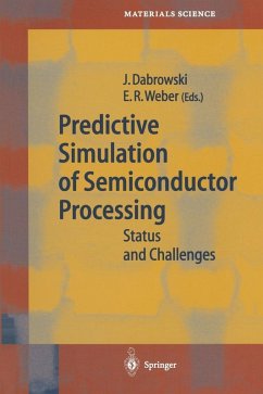
Predictive simulation of semiconductor processing enables researchers and developers to extend the scaling range of semiconductor devices beyond the parameter range of empirical research. It requires a thorough understanding of the basic mechanisms employed in device fabrication, such as diffusion, ion implantation, epitaxy, defect formation and annealing, and contamination. This book presents an in-depth discussion of our current understanding of key processes and identifies areas that require further work in order to achieve the goal of a comprehensive, predictive process simulation tool.

  • Geräte: PC
  • ohne Kopierschutz
  • eBook Hilfe
  • Größe: 50.25MB
Produktbeschreibung
Predictive simulation of semiconductor processing enables researchers and developers to extend the scaling range of semiconductor devices beyond the parameter range of empirical research. It requires a thorough understanding of the basic mechanisms employed in device fabrication, such as diffusion, ion implantation, epitaxy, defect formation and annealing, and contamination. This book presents an in-depth discussion of our current understanding of key processes and identifies areas that require further work in order to achieve the goal of a comprehensive, predictive process simulation tool.


Dieser Download kann aus rechtlichen Gründen nur mit Rechnungsadresse in A, B, BG, CY, CZ, D, DK, EW, E, FIN, F, GR, HR, H, IRL, I, LT, L, LR, M, NL, PL, P, R, S, SLO, SK ausgeliefert werden.

Autorenporträt
J. Dabrowski: Born in Warsaw, Poland, Sept. 29, 1958. PhD, Institute of Physics of the Polish Academy of Science (IF PAN), Warsaw, 1989. Scientific staff member IF PAN 1983-1992; postdoctoral fellow Fritz Haber Inbstitute of the Max Planck Society, Berlin, Germany, 1990-1991; postdoctoral fellow Xerox Palo Alto Research Center, California, 1992; since 1993 with IHP-microelectronics, Frankfurt (Oder), Germany. Conference series chairman, Challenges in Predictive Process Simulation (1997, 2000, 2002); international advisory commmittee member, International Training Institute for Materials Science, Hanoi, Vietnam. Project leader, German Research Society (1998-2000); von Neuman Institute for Computing (since 1993). Author (monograph), "Silicon surfaces and formation of interfaces; basic science in the industrial world" (World Scientific, 2000). Editor (book) , ""Recent Developments in Vacuum Science and Technology" (Research Signpost, 2003). Research in atomic diffusion mechanism in solid state; atomic structure of surfaces and semiconductor/dielectric interfaces; atomic structure of defects in semiconductors and insulators; signal processing for telecommunication. Achievements include discovery of atomic structure of the clean Si(113) surface; atomic structure of the main electron trap in GaAs (EL2 defect); atomic structure of the interface between a high-K dielectric (Pr2O3) and Si(001). Patents for silicon microelectronic technology; patents pending for telecommunication.
Rezensionen
From the reviews:

"This book presents an in-depth discussion of our current understanding of key processes and identifies areas that require further work in order to achieve the goal of a comprehensive, predictive process simulation tool. Eleven contributions make up the book; each is supported by a wealth of references. ... A valuable reference and guide to have on the shelf for frequent use and study. Certainly, the expertise and research experience of the contributors cannot be questioned. Summing up ... a richly rewarding work." (Current Engineering Practice, Vol. 47 (3), 2004-2005)