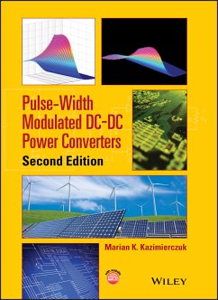
Pulse-Width Modulated DC-DC Power Converters (eBook, PDF)


Alle Infos zum eBook verschenken

Pulse-Width Modulated DC-DC Power Converters (eBook, PDF)
- Format: PDF
- Merkliste
- Auf die Merkliste
- Bewerten Bewerten
- Teilen
- Produkt teilen
- Produkterinnerung
- Produkterinnerung

Hier können Sie sich einloggen

Bitte loggen Sie sich zunächst in Ihr Kundenkonto ein oder registrieren Sie sich bei bücher.de, um das eBook-Abo tolino select nutzen zu können.
PWM DC-DC power converter technology underpins many energy conversion systems including renewable energy circuits, active power factor correctors, battery chargers, portable devices and LED drivers. Following the success of Pulse-Width Modulated DC-DC Power Converters this second edition has been thoroughly revised and expanded to cover the latest challenges and advances in the field. Key features of 2nd edition: * Four new chapters, detailing the latest advances in power conversion, focus on: small-signal model and dynamic characteristics of the buck converter in continuous conduction mode;…mehr
- Geräte: PC
- mit Kopierschutz
- eBook Hilfe
- Größe: 39.07MB
![Pulse-width Modulated DC-DC Power Converters (eBook, PDF) Pulse-width Modulated DC-DC Power Converters (eBook, PDF)]() Marian K. KazimierczukPulse-width Modulated DC-DC Power Converters (eBook, PDF)128,99 €
Marian K. KazimierczukPulse-width Modulated DC-DC Power Converters (eBook, PDF)128,99 €![Laboratory Manual for Pulse-Width Modulated DC-DC Power Converters (eBook, PDF) Laboratory Manual for Pulse-Width Modulated DC-DC Power Converters (eBook, PDF)]() Marian K. KazimierczukLaboratory Manual for Pulse-Width Modulated DC-DC Power Converters (eBook, PDF)49,99 €
Marian K. KazimierczukLaboratory Manual for Pulse-Width Modulated DC-DC Power Converters (eBook, PDF)49,99 €![Pulse-Width Modulated DC-DC Power Converters (eBook, ePUB) Pulse-Width Modulated DC-DC Power Converters (eBook, ePUB)]() Marian K. KazimierczukPulse-Width Modulated DC-DC Power Converters (eBook, ePUB)115,99 €
Marian K. KazimierczukPulse-Width Modulated DC-DC Power Converters (eBook, ePUB)115,99 €![Pulse Width Modulated DC-DC Converters (eBook, PDF) Pulse Width Modulated DC-DC Converters (eBook, PDF)]() Keng Chih WuPulse Width Modulated DC-DC Converters (eBook, PDF)113,95 €
Keng Chih WuPulse Width Modulated DC-DC Converters (eBook, PDF)113,95 €![Pulsewidth Modulated DC-to-DC Power Conversion (eBook, PDF) Pulsewidth Modulated DC-to-DC Power Conversion (eBook, PDF)]() Byungcho ChoiPulsewidth Modulated DC-to-DC Power Conversion (eBook, PDF)122,99 €
Byungcho ChoiPulsewidth Modulated DC-to-DC Power Conversion (eBook, PDF)122,99 €![Transients of Modern Power Electronics (eBook, PDF) Transients of Modern Power Electronics (eBook, PDF)]() Hua BaiTransients of Modern Power Electronics (eBook, PDF)110,99 €
Hua BaiTransients of Modern Power Electronics (eBook, PDF)110,99 €![Average Current-Mode Control of DC-DC Power Converters (eBook, PDF) Average Current-Mode Control of DC-DC Power Converters (eBook, PDF)]() Marian K. KazimierczukAverage Current-Mode Control of DC-DC Power Converters (eBook, PDF)123,99 €
Marian K. KazimierczukAverage Current-Mode Control of DC-DC Power Converters (eBook, PDF)123,99 €-
-
-
Dieser Download kann aus rechtlichen Gründen nur mit Rechnungsadresse in A, B, BG, CY, CZ, D, DK, EW, E, FIN, F, GR, HR, H, IRL, I, LT, L, LR, M, NL, PL, P, R, S, SLO, SK ausgeliefert werden.
- Produktdetails
- Verlag: John Wiley & Sons
- Seitenzahl: 960
- Erscheinungstermin: 13. August 2015
- Englisch
- ISBN-13: 9781119009566
- Artikelnr.: 43665660
- Verlag: John Wiley & Sons
- Seitenzahl: 960
- Erscheinungstermin: 13. August 2015
- Englisch
- ISBN-13: 9781119009566
- Artikelnr.: 43665660
- Herstellerkennzeichnung Die Herstellerinformationen sind derzeit nicht verfügbar.
DT 25 2.2.4 Time Interval: DT < t
T 26 2.2.5 Device Stresses for CCM 27 2.2.6 DC Voltage Transfer Function for CCM 27 2.2.7 Boundary Between CCM and DCM 29 2.2.8 Capacitors 31 2.2.9 Ripple Voltage in Buck Converter for CCM 33 2.2.10 Switching Losses with Linear MOSFET Output Capacitance 39 2.2.11 Switching Losses with Nonlinear MOSFET Output Capacitance 40 2.2.12 Power Losses and Efficiency of Buck Converter for CCM 43 2.2.13 DC Voltage Transfer Function of Lossy Converter for CCM 48 2.2.14 MOSFET Gate-Drive Power 48 2.2.15 Gate Driver 49 2.2.16 Design of Buck Converter for CCM 50 2.3 DC Analysis of PWM Buck Converter for DCM 52 2.3.1 Time Interval: 0 < t
DT 56 2.3.2 Time Interval: DT < t
(D + D1)T 58 2.3.3 Time Interval: (D + D1)T < t
T 58 2.3.4 Device Stresses for DCM 59 2.3.5 DC Voltage Transfer Function for DCM 59 2.3.6 Maximum Inductance for DCM 62 2.3.7 Power Losses and Efficiency of Buck Converter for DCM 63 2.3.8 Design of Buck Converter for DCM 65 2.4 Buck Converter with Input Filter 68 2.5 Buck Converter with Synchronous Rectifier 68 2.6 Buck Converter with Positive Common Rail 76 2.7 Quadratic Buck Converter 76 2.8 Tapped-Inductor Buck Converters 79 2.8.1 Tapped-Inductor Common-Diode Buck Converter 79 2.8.2 Tapped-Inductor Common-Transistor Buck Converter 81 2.8.3 Watkins-Johnson Converter 82 2.9 Multiphase Buck Converter 83 2.10 Switched-Inductor Buck Converter 85 2.11 Layout 85 2.12 Summary 85 References 87 Review Questions 88 Problems 88 3 Boost PWM DC-DC Converter 90 3.1 Introduction 90 3.2 DC Analysis of PWM Boost Converter for CCM 90 3.2.1 Circuit Description 90 3.2.2 Assumptions 91 3.2.3 Time Interval: 0 < t
DT 93 3.2.4 Time Interval: DT < t
T 94 3.2.5 DC Voltage Transfer Function for CCM 94 3.2.6 Boundary Between CCM and DCM 95 3.2.7 Ripple Voltage in Boost Converter for CCM 98 3.2.8 Power Losses and Efficiency of Boost Converter for CCM 100 3.2.9 DC Voltage Transfer Function of Lossy Boost Converter for CCM 102 3.2.10 Design of Boost Converter for CCM 103 3.3 DC Analysis of PWM Boost Converter for DCM 107 3.3.1 Time Interval: 0 < t
DT 110 3.3.2 Time Interval: DT < t
(D + D1)T 111 3.3.3 Time Interval: (D + D1)T < t
T 112 3.3.4 Device Stresses for DCM 112 3.3.5 DC Voltage Transfer Function for DCM 112 3.3.6 Maximum Inductance for DCM 117 3.3.7 Power Losses and Efficiency of Boost Converter for DCM 117 3.3.8 Design of Boost Converter for DCM 120 3.4 Bidirectional Buck and Boost Converters 127 3.5 Synchronous Boost Converter 129 3.6 Tapped-Inductor Boost Converters 129 3.6.1 Tapped-Inductor Common-Diode Boost Converter 131 3.6.2 Tapped-Inductor Common-Load Boost Converter 132 3.7 Duality 133 3.8 Power Factor Correction 134 3.8.1 Power Factor 134 3.8.2 Boost Power Factor Corrector 138 3.8.3 Electronic Ballasts for Fluorescent Lamps 141 3.9 Summary 141 References 142 Review Questions 143 Problems 143 4 Buck-Boost PWM DC-DC Converter 145 4.1 Introduction 145 4.2 DC Analysis of PWM Buck-Boost Converter for CCM 145 4.2.1 Circuit Description 145 4.2.2 Assumptions 146 4.2.3 Time Interval: 0 < t
DT 146 4.2.4 Time Interval: DT < t
T 148 4.2.5 DC Voltage Transfer Function for CCM 149 4.2.6 Device Stresses for CCM 150 4.2.7 Boundary Between CCM and DCM 151 4.2.8 Ripple Voltage in Buck-Boost Converter for CCM 152 4.2.9 Power Losses and Efficiency of the Buck-Boost Converter for CCM 155 4.2.10 DC Voltage Transfer Function of Lossy Buck-Boost Converter for CCM 158 4.2.11 Design of Buck-Boost Converter for CCM 159 4.3 DC Analysis of PWM Buck-Boost Converter for DCM 162 4.3.1 Time Interval: 0 < t
DT 165 4.3.2 Time Interval: DT < t
(D + D1)T 166 4.3.3 Time Interval: (D + D1)T < t
T 167 4.3.4 Device Stresses of the Buck-Boost Converter in DCM 167 4.3.5 DC Voltage Transfer Function of the Buck-Boost Converter for DCM 167 4.3.6 Maximum Inductance for DCM 170 4.3.7 Power Losses and Efficiency of the Buck-Boost Converter in DCM 172 4.3.8 Design of Buck-Boost Converter for DCM 174 4.4 Bidirectional Buck-Boost Converter 180 4.5 Synthesis of Buck-Boost Converter 181 4.6 Synthesis of Boost-Buck (
uk) Converter 183 4.7 Noninverting Buck-Boost Converters 184 4.7.1 Cascaded Noninverting Buck-Boost Converters 184 4.7.2 Four-Transistor Noninverting Buck-Boost Converters 184 4.8 Tapped-Inductor Buck-Boost Converters 186 4.8.1 Tapped-Inductor Common-Diode Buck-Boost Converter 186 4.8.2 Tapped-Inductor Common-Transistor Buck-Boost Converter 187 4.8.3 Tapped-Inductor Common-Load Buck-Boost Converter 188 4.8.4 Tapped-Inductor Common-Source Buck-Boost Converter 191 4.9 Summary 192 References 192 Review Questions 193 Problems 193 5 Flyback PWM DC-DC Converter 195 5.1 Introduction 195 5.2 Transformers 196 5.3 DC Analysis of PWM Flyback Converter for CCM 197 5.3.1 Derivation of PWM Flyback Converter 197 5.3.2 Circuit Description 197 5.3.3 Assumptions 199 5.3.4 Time Interval: 0 < t
DT 200 5.3.5 Time Interval: DT < t
T 201 5.3.6 DC Voltage Transfer Function for CCM 203 5.3.7 Boundary Between CCM and DCM 204 5.3.8 Ripple Voltage in Flyback Converter for CCM 205 5.3.9 Power Losses and Efficiency of Flyback Converter for CCM 207 5.3.10 DC Voltage Transfer Function of Lossy Converter for CCM 210 5.3.11 Design of Flyback Converter for CCM 211 5.4 DC Analysis of PWM Flyback Converter for DCM 214 5.4.1 Time Interval: 0 < t
DT 217 5.4.2 Time Interval: DT < t
(D + D1)T 219 5.4.3 Time Interval: (D + D1)T < t
T 220 5.4.4 DC Voltage Transfer Function for DCM 221 5.4.5 Maximum Magnetizing Inductance for DCM 222 5.4.6 Ripple Voltage in Flyback Converter for DCM 225 5.4.7 Power Losses and Efficiency of Flyback Converter for DCM 226 5.4.8 Design of Flyback Converter for DCM 228 5.5 Multiple-Output Flyback Converter 232 5.6 Bidirectional Flyback Converter 237 5.7 Ringing in Flyback Converter 237 5.8 Flyback Converter with Passive Dissipative Snubber 240 5.9 Flyback Converter with Zener Diode Voltage Clamp 240 5.10 Flyback Converter with Active Clamping 241 5.11 Two-Transistor Flyback Converter 241 5.12 Summary 243 References 244 Review Questions 244 Problems 245 6 Forward PWM DC-DC Converter 246 6.1 Introduction 246 6.2 DC Analysis of PWM Forward Converter for CCM 246 6.2.1 Derivation of Forward PWM Converter 246 6.2.2 Time Interval: 0 < t
DT 248 6.2.3 Time Interval: DT < t
DT + tm 251 6.2.4 Time Interval: DT + tm < t
T 253 6.2.5 Maximum Duty Cycle 253 6.2.6 Device Stresses 254 6.2.7 DC Voltage Transfer Function for CCM 255 6.2.8 Boundary Between CCM and DCM 255 6.2.9 Ripple Voltage in Forward Converter for CCM 256 6.2.10 Power Losses and Efficiency of Forward Converter for CCM 258 6.2.11 DC Voltage Transfer Function of Lossy Converter for CCM 261 6.2.12 Design of Forward Converter for CCM 262 6.3 DC Analysis of PWM Forward Converter for DCM 269 6.3.1 Time Interval: 0 < t
DT 269 6.3.2 Time Interval: DT < t
DT + tm 272 6.3.3 Time Interval: DT + tm < t
(D + D1)T 273 6.3.4 Time Interval: (D + D1)T < t
T 273 6.3.5 DC Voltage Transfer Function for DCM 274 6.3.6 Maximum Inductance for DCM 277 6.3.7 Power Losses and Efficiency of Forward Converter for DCM 278 6.3.8 Design of Forward Converter for DCM 280 6.4 Multiple-Output Forward Converter 288 6.5 Forward Converter with Synchronous Rectifier 288 6.6 Forward Converters with Active Clamping 288 6.7 Two-Switch Forward Converter 290 6.8 Forward-Flyback Converter 291 6.9 Summary 292 References 293 Review Questions 293 Problems 294 7 Half-Bridge PWM DC-DC Converter 296 7.1 Introduction 296 7.2 DC Analysis of PWM Half-Bridge Converter for CCM 296 7.2.1 Circuit Description 296 7.2.2 Assumptions 299 7.2.3 Time Interval: 0 < t
DT 299 7.2.4 Time Interval: DT < t
T
2 301 7.2.5 Time Interval: T
2 < t
T
2 + DT 303 7.2.6 Time Interval: T
2 + DT < t
T 304 7.2.7 Device Stresses 304 7.2.8 DC Voltage Transfer Function of Lossless Half-Bridge Converter for CCM 304 7.2.9 Boundary Between CCM and DCM 305 7.2.10 Ripple Voltage in Half-Bridge Converter for CCM 306 7.2.11 Power Losses and Efficiency of Half-Bridge Converter for CCM 308 7.2.12 DC Voltage Transfer Function of Lossy Converter for CCM 311 7.2.13 Design of Half-Bridge Converter for CCM 312 7.3 DC Analysis of PWM Half-Bridge Converter for DCM 315 7.3.1 Time Interval: 0 < t
DT 315 7.3.2 Time Interval: DT < t
(D + D1)T 320 7.3.3 Time Interval: (D + D1)T < t
T
2 322 7.3.4 DC Voltage Transfer Function for DCM 322 7.3.5 Maximum Inductance for DCM 326 7.4 Summary 326 References 327 Review Questions 327 Problems 328 8 Full-Bridge PWM DC-DC Converter 330 8.1 Introduction 330 8.2 DC Analysis of PWM Full-Bridge Converter for CCM 330 8.2.1 Circuit Description 330 8.2.2 Assumptions 332 8.2.3 Time Interval: 0 < t
DT 332 8.2.4 Time Interval: DT < t
T
2 334 8.2.5 Time Interval: T
2 < t
T
2 + DT 336 8.2.6 Time Interval: T
2 + DT < t
T 336 8.2.7 Device Stresses 337 8.2.8 DC Voltage Transfer Function of Lossless Full-Wave Converter for CCM 337 8.2.9 Boundary Between CCM and DCM 338 8.2.10 Ripple Voltage in Full-Bridge Converter for CCM 339 8.2.11 Power Losses and Efficiency of Full-Bridge Converter for CCM 340 8.2.12 DC Voltage Transfer Function of Lossy Converter for CCM 344 8.2.13 Design of Full-Bridge Converter for CCM 345 8.3 DC Analysis of PWM Full-Bridge Converter for DCM 351 8.3.1 Time Interval: 0 < t
DT 351 8.3.2 Time Interval: DT < t
(D + D1)T 353 8.3.3 Time Interval: (D + D1)T < t
T
2 355 8.3.4 DC Voltage Transfer Function for DCM 356 8.3.5 Maximum Inductance for DCM 359 8.4 Phase-Controlled Full-Bridge Converter 361 8.5 Summary 362 References 362 Review Questions 362 Problems 363 9 Small-Signal Models of PWM Converters for CCM and DCM 365 9.1 Introduction 365 9.2 Assumptions 366 9.3 Averaged Model of Ideal Switching Network for CCM 366 9.4 Averaged Values of Switched Resistances 369 9.5 Model Reduction 375 9.6 Large-Signal Averaged Model for CCM 377 9.7 DC and Small-Signal Circuit Linear Models of Switching Network for CCM 381 9.7.1 Large-Signal Circuit Model of Switching Network for CCM 381 9.7.2 Linearization of Switching Network Model for CCM 384 9.8 Block Diagram of Small-signal Model of PWM DC-DC Converters 385 9.9 Family of PWM Converter Models for CCM 386 9.10 PWM Small-Signal Switch Model for CCM 389 9.11 Modeling of Ideal Switching Network for DCM 391 9.11.1 Relationships Among DC Components for DCM 391 9.11.2 Small-Signal Model of Ideal Switching Network for DCM 395 9.12 Averaged Parasitic Resistances for DCM 398 9.13 Summary 400 References 402 Review Questions 405 Problems 405 10 Small-Signal Characteristics of Buck Converter for CCM 407 10.1 Introduction 407 10.2 Small-Signal Model of the PWM Buck Converter 407 10.3 Open-Loop Transfer Functions 408 10.3.1 Open-Loop Control-to-Output Transfer Function 409 10.3.2 Delay in Control-to-Output Transfer Function 416 10.3.3 Open-Loop Input-to-Output Transfer Function 418 10.3.4 Open-Loop Input Impedance 420 10.3.5 Open-Loop Output Impedance 423 10.4 Open-Loop Step Responses 426 10.4.1 Open-Loop Response of Output Voltage to Step Change in Input Voltage 426 10.4.2 Open-Loop Response of Output Voltage to Step Change in Duty Cycle 431 10.4.3 Open-Loop Response of Output Voltage to Step Change in Load Current 433 10.5 Open-Loop DC Transfer Functions 434 10.6 Summary 436 References 436 Review Questions 437 Problems 438 11 Small-Signal Characteristics of Boost Converter for CCM 439 11.1 Introduction 439 11.2 DC Characteristics 439 11.3 Open-Loop Control-to-Output Transfer Function 440 11.4 Delay in Open-Loop Control-to-Output Transfer Function 449 11.5 Open-Loop Audio Susceptibility 451 11.6 Open-Loop Input Impedance 455 11.7 Open-Loop Output Impedance 457 11.8 Open-Loop Step Responses 461 11.8.1 Open-Loop Response of Output Voltage to Step Change in Input Voltage 461 11.8.2 Open-Loop Response of Output Voltage to Step Change in Duty Cycle 464 11.8.3 Open-Loop Response of Output Voltage to Step Change in Load Current 465 11.9 Summary 467 References 467 Review Questions 468 Problems 468 12 Voltage-Mode Control of PWM Buck Converter 470 12.1 Introduction 470 12.2 Properties of Negative Feedback 471 12.3 Stability 474 12.4 Single-Loop Control of PWM Buck Converter 475 12.5 Closed-Loop Small-Signal Model of Buck Converter 478 12.6 Pulse-Width Modulator 478 12.7 Feedback Network 483 12.8 Transfer Function of Buck Converter with Modulator and Feedback Network 486 12.9 Control Circuits 489 12.9.1 Error Amplifier 489 12.9.2 Proportional Controller 490 12.9.3 Integral Controller 492 12.9.4 Proportional-Integral Controller 493 12.9.5 Integral-Single-Lead Controller 497 12.9.6 Loop Gain 504 12.9.7 Closed-Loop Control-to-Output Voltage Transfer Function 504 12.9.8 Closed-Loop Input-to-Output Transfer Function 506 12.9.9 Closed-Loop Input Impedance 508 12.9.10 Closed-Loop Output Impedance 509 12.10 Closed-Loop Step Responses 511 12.10.1 Response to Step Change in Input Voltage 511 12.10.2 Response to Step Change in Reference Voltage 513 12.10.3 Closed-Loop Response to Step Change in Load Current 515 12.10.4 Closed-Loop DC Transfer Functions 515 12.11 Summary 518 References 519 Review Questions 519 Problems 520 13 Voltage-Mode Control of Boost Converter 521 13.1 Introduction 521 13.2 Circuit of Boost Converter with Voltage-Mode Control 521 13.3 Transfer Function of Modulator, Boost Converter Power Stage, and Feedback Network 523 13.4 Integral-Double-Lead Controller 527 13.5 Design of Integral-Double-Lead Controller 532 13.6 Loop Gain 536 13.7 Closed-Loop Control-to-Output Voltage Transfer Function 537 13.8 Closed-Loop Audio Susceptibility 539 13.9 Closed-Loop Input Impedance 539 13.10 Closed-Loop Output Impedance 542 13.11 Closed-Loop Step Responses 544 13.11.1 Closed-Loop Response to Step Change in Input Voltage 544 13.11.2 Closed-Loop Response to Step Change in Reference Voltage 547 13.11.3 Closed-Loop Response to Step Change in Load Current 548 13.12 Closed-Loop DC Transfer Functions 549 13.13 Summary 552 References 552 Review Questions 552 Problems 553 14 Current-Mode Control 554 14.1 Introduction 554 14.2 Principle of Operation of PWM Converters with Peak CMC 555 14.3 Relationship Between Duty Cycle and Inductor-Current Slopes 559 14.4 Instability of Closed-Current Loop 560 14.5 Slope Compensation 564 14.5.1 Analysis of Slope Compensation in Time Domain 564 14.5.2 Boundary of Slope Compensation for Buck and Buck-Boost Converters 569 14.5.3 Boundary Slope Compensation for Boost Converter 570 14.6 Sample-and-Hold Effect on Current Loop 570 14.6.1 Natural Response of Inductor Current to Small Perturbation in Closed-Current Loop 572 14.6.2 Forced Response of Inductor Current to Step Change in Control Voltage in Closed-Current Loop 575 14.6.3 Relationship Between s-Domain and z-Domain 577 14.6.4 Transfer Function of Closed-Current Loop in z-Domain 578 14.7 Closed-Loop Control Voltage-to-Inductor Current Transfer Function in s-Domain 580 14.7.1 Approximation of Hicl by Rational Transfer Function 582 14.7.2 Step Responses of Closed-Inner Loop 588 14.8 Loop Gain of Current Loop 588 14.8.1 Loop Gain of Inner Loop in z-Domain 588 14.8.2 Loop Gain of Inner Loop in s-Domain 590 14.9 Gain-Crossover Frequency of Inner Loop 595 14.10 Phase Margin of Inner Loop 596 14.11 Maximum Duty Cycle for Converters without Slope Compensation 598 14.12 Maximum Duty Cycle for Converters with Slope Compensation 600 14.13 Minimum Slope Compensation for Buck and Buck-Boost Converter 605 14.14 Minimum Slope Compensation for Boost Converter 607 14.15 Error Voltage-to-Duty Cycle Transfer Function 610 14.16 Closed-Loop Control Voltage-to-Duty Cycle Transfer Function of Current Loop 614 14.17 Alternative Representation of Current Loop 618 14.18 Current Loop with Disturbances 618 14.18.1 Modified Approximation of Current Loop 619 14.19 Voltage Loop of PWM Converters with Current-Mode Control 624 14.19.1 Control-to-Output Transfer Function for Buck Converter 624 14.19.2 Block Diagram of Power Stages of PWM Converters 627 14.19.3 Closed-Voltage Loop Transfer Function of PWM Converters with Current-Mode Control 628 14.19.4 Closed-Loop Audio Susceptibility of PWM Converters with Current-Mode Control 628 14.19.5 Closed-Loop Output Impedance of PWM Converters with Current-Mode Control 630 14.20 Feedforward Gains in PWM Converters with Current-Mode Control without Slope Compensation 631 14.21 Feedforward Gains in PWM Converters with Current-Mode Control and Slope Compensation 634 14.22 Control-to-Output Voltage Transfer Function of Inner Loop with Feedforward Gains 636 14.23 Audio-Susceptibility of Inner Loop with Feedforward Gains 637 14.24 Closed-Loop Transfer Functions with Feedforward Gains 638 14.25 Slope Compensation by Adding a Ramp to Inductor Current Waveform 638 14.26 Relationships for Constant-Frequency Current-Mode On-Time Control 639 14.27 Summary 639 References 640 Review Questions 644 Problems 644 14.28 Appendix: Sample-and-Hold Modeling 645 14.28.1 Sampler of the Control Voltage 645 14.28.2 Zero-Order Hold of Inductor Current 648 14.28.3 Approximations of esTs 650 15 Current-Mode Control of Boost Converter 653 15.1 Introduction 653 15.2 Open-Loop Small-Signal Transfer Functions 653 15.2.1 Open-Loop Duty Cycle-to-Inductor Current Transfer Function 653 15.2.2 High-Frequency Open-Loop Duty Cycle-to-Inductor Current Transfer Function 659 15.2.3 Open-Loop Input Voltage-to-Inductor Current Transfer Function 660 15.2.4 Open-Loop Inductor-to-Output Current Transfer Function 665 15.3 Open-Loop Step Responses of Inductor Current 667 15.3.1 Open-Loop Response of Inductor Current to Step Change in Input Voltage 667 15.3.2 Open-Loop Response of the Inductor Current to Step Change in the Duty Cycle 670 15.3.3 Open-Loop Response of Inductor Current to Step Change in Load Current 672 15.4 Closed-Current-Loop Transfer Functions 675 15.4.1 Forward Gain 675 15.4.2 Loop Gain of Current Loop 675 15.4.3 Closed-Loop Gain of Current Loop 675 15.4.4 Control-to-Output Transfer Function 677 15.4.5 Input Voltage-to-Duty Cycle Transfer Function 684 15.4.6 Load Current-to-Duty Cycle Transfer Function 688 15.4.7 Output Impedance of Closed-Current Loop 690 15.5 Closed-Voltage-Loop Transfer Functions 695 15.5.1 Control-to-Output Transfer Function 695 15.5.2 Control Voltage-to-Feedback Voltage Transfer Function 695 15.5.3 Loop Gain of Voltage Loop 697 15.5.4 Closed-Loop Gain of Voltage Loop 701 15.5.5 Closed-Loop Audio Susceptibility with Integral Controller 703 15.5.6 Closed-Loop Output Impedance with Integral Controller 704 15.6 Closed-Loop Step Responses 706 15.6.1 Closed-Loop Response of Output Voltage to Step Change in Input Voltage 706 15.6.2 Closed-Loop Response of Output Voltage to Step Change in Load Current 708 15.6.3 Closed-Loop Response of Output Voltage to Step Change in Reference Voltage 708 15.7 Closed-Loop DC Transfer Functions 710 15.8 Summary 711 References 711 Review Questions 712 Problems 712 16 Open-Loop Small-Signal Characteristics of PWM Boost Converter for DCM 713 16.1 Introduction 713 16.2 Small-Signal Model of Boost Converter for DCM 713 16.3 Open-Loop Control-to-Output Transfer Function 716 16.4 Open-Loop Input-to-Output Voltage Transfer Function 719 16.5 Open-Loop Input Impedance 724 16.6 Open-Loop Output Impedance 725 16.7 Step Responses of Output Voltage of Boost Converter for DCM 728 16.7.1 Response of Output Voltage to Step Change in Input Voltage 728 16.7.2 Response of Output Voltage to Step Change in Duty Cycle 730 16.7.3 Response of Output Voltage to Step Change in Load Current 730 16.8 Open-Loop Duty Cycle-to-Inductor Current Transfer Function 731 16.9 Open-Loop Input Voltage-to-Inductor Current Transfer Function 735 16.10 Open-Loop Output Current-to-Inductor Current Transfer Function 735 16.11 Step Responses of Inductor Current of Boost Converter for DCM 738 16.11.1 Step Response of Inductor Current to Step Change in Input Voltage 738 16.11.2 Step Response of Inductor Current to Step Change in Duty Cycle 740 16.11.3 Step Response of Inductor Current to Step Change in Load Current 741 16.12 DC Characteristics of Boost Converter for DCM 742 16.12.1 DC-to-DC Voltage Transfer Function of Lossless Boost Converter for DCM 742 16.12.2 DC-to-DC Voltage Transfer Function of Lossy Boost Converter for DCM 743 16.12.3 Efficiency of Boost Converter for DCM 745 16.13 Summary 745 References 745 Review Questions 746 Problems 746 17 Silicon and Silicon-Carbide Power Diodes 747 17.1 Introduction 747 17.2 Electronic Power Switches 747 17.3 Atom 748 17.4 Electron and Hole Effective Mass 749 17.5 Semiconductors 750 17.6 Intrinsic Semiconductors 751 17.7 Extrinsic Semiconductors 756 17.7.1 n-Type Semiconductor 756 17.7.2 p-Type Semiconductor 759 17.7.3 Maximum Operating Temperature 761 17.8 Wide Band Gap Semiconductors 762 17.9 Physical Structure of Junction Diodes 764 17.9.1 Formation of Depletion Layer 765 17.9.2 Charge Transport 767 17.10 Static I-V Diode Characteristic 768 17.11 Breakdown Voltage of Junction Diodes 772 17.11.1 Depletion-Layer Width 773 17.11.2 Electric Field Intensity Distribution 775 17.11.3 Avalanche Breakdown Voltage 779 17.11.4 Punch-Through Breakdown Voltage 781 17.11.5 Edge Terminations 782 17.12 Capacitances of Junction Diodes 784 17.12.1 Junction Capacitance 784 17.12.2 Diffusion Capacitance 787 17.13 Reverse Recovery of pn Junction Diodes 789 17.13.1 Qualitative Description 789 17.13.2 Reverse Recovery in Resistive Circuits 790 17.13.3 Charge-Continuity Equation 793 17.13.4 Reverse Recovery in Inductive Circuits 796 17.14 Schottky Diodes 798 17.14.1 Static I-V Characteristic of Schottky Diodes 801 17.14.2 Breakdown Voltages of Schottky Diodes 802 17.14.3 Junction Capacitance of Schottky Diodes 802 17.14.4 Switching Characteristics of Schottky Diodes 802 17.15 Solar Cells 806 17.16 Light-Emitting Diodes 809 17.17 SPICE Model of Diodes 810 17.18 Summary 811 References 815 Review Questions 816 Problems 817 18 Silicon and Silicon-Carbide Power MOSFETs 819 18.1 Introduction 819 18.2 Integrated MOSFETs 819 18.3 Physical Structure of Power MOSFETs 819 18.4 Principle of Operation of Power MOSFETs 824 18.4.1 Cutoff Region 824 18.4.2 Formation of MOSFET Channel 824 18.4.3 Linear Region 824 18.4.4 Saturation Region 825 18.4.5 Antiparallel Diode 825 18.5 Derivation of Power MOSFET Characteristics 826 18.5.1 Ohmic Region 826 18.5.2 Pinch-off Region 829 18.5.3 Channel-Length Modulation 830 18.6 Power MOSFET Characteristics 831 18.7 Mobility of Charge Carr
