73,95 €
73,95 €
inkl. MwSt.
Sofort per Download lieferbar
payback
37 °P sammeln
73,95 €
73,95 €
inkl. MwSt.
Sofort per Download lieferbar

Alle Infos zum eBook verschenken
payback
37 °P sammeln
Als Download kaufen
73,95 €
inkl. MwSt.
Sofort per Download lieferbar
payback
37 °P sammeln
Jetzt verschenken
73,95 €
inkl. MwSt.
Sofort per Download lieferbar

Alle Infos zum eBook verschenken
payback
37 °P sammeln
  • Format: PDF

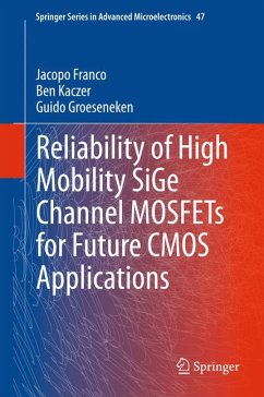
Due to the ever increasing electric fields in scaled CMOS devices, reliability is becoming a showstopper for further scaled technology nodes. Although several groups have already demonstrated functional Si channel devices with aggressively scaled Equivalent Oxide Thickness (EOT) down to 5Å, a 10 year reliable device operation cannot be guaranteed anymore due to severe Negative Bias Temperature Instability.
This book focuses on the reliability of the novel (Si)Ge channel quantum well pMOSFET technology. This technology is being considered for possible implementation in next CMOS technology
…mehr

Produktbeschreibung
Due to the ever increasing electric fields in scaled CMOS devices, reliability is becoming a showstopper for further scaled technology nodes. Although several groups have already demonstrated functional Si channel devices with aggressively scaled Equivalent Oxide Thickness (EOT) down to 5Å, a 10 year reliable device operation cannot be guaranteed anymore due to severe Negative Bias Temperature Instability.

This book focuses on the reliability of the novel (Si)Ge channel quantum well pMOSFET technology. This technology is being considered for possible implementation in next CMOS technology nodes, thanks to its benefit in terms of carrier mobility and device threshold voltage tuning. We observe that it also opens a degree of freedom for device reliability optimization. By properly tuning the device gate stack, sufficiently reliable ultra-thin EOT devices with a 10 years lifetime at operating conditions are demonstrated.

The extensive experimental datasets collected on a variety of processed 300mm wafers and presented here show the reliability improvement to be process- and architecture-independent and, as such, readily transferable to advanced device architectures as Tri-Gate (finFET) devices. We propose a physical model to understand the intrinsically superior reliability of the MOS system consisting of a Ge-based channel and a SiO2/HfO2 dielectric stack.

The improved reliability properties here discussed strongly support (Si)Ge technology as a clear frontrunner for future CMOS technology nodes.


Dieser Download kann aus rechtlichen Gründen nur mit Rechnungsadresse in A, B, BG, CY, CZ, D, DK, EW, E, FIN, F, GR, HR, H, IRL, I, LT, L, LR, M, NL, PL, P, R, S, SLO, SK ausgeliefert werden.

Autorenporträt
Jacopo Franco received the M.Sc. in Electronic Engineering from Università della Calabria, Italy, in 2008 and the Ph.D. degree in Engineering from the KU Leuven, Belgium, in 2013. He is currently a Researcher in the reliability group of imec, Leuven, Belgium. His research interests focus on the reliability of high-mobility channel transistors for future CMOS nodes and on variability issues in nanoscale devices. He has co-authored more than 70 papers in international journal and conference proceedings and received the Best Student Paper Award at SISC (2009), the EDS Ph.D. Student Fellowship (2012), the EDS Paul Rappaport Award (2011), and the Best Paper Award at IRPS (2012).

Ben Kaczer is a Principal Scientist at imec, Belgium. He received the M.S. degree in Physical Electronics from Charles University, Prague, in 1992 and the M.S. and Ph.D. degrees in Physics from The Ohio State University, in 1996 and 1998, respectively. In 1998 he joined the reliability group of imec. He has co-authored more than 300 papers and received 5 Best or Outstanding IRPS and 1 IPFA Paper Awards. He is currently serving on the IEEE T. Electron Dev. Editorial Board.

Guido Groeseneken received the M.Sc. degree in 1980 and the Ph.D degree in applied sciences in 1986, both from the KU Leuven, Belgium. In 1987 he joined the R&D Laboratory of imec, Leuven, Belgium, where he is responsible for research in reliability physics for deep submicron CMOS technologies and in nanotechnology for post-CMOS applications. Since 2001 he is Professor at the KU Leuven, where he is Program Director of the Master in Nanoscience and Nanotechnology and coordinating a European Erasmus Mundus Master program in Nanoscience and nanotechnology. He became an IEEE Fellow in 2005 and an IMEC Fellow in 2007.