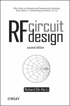
RF Circuit Design (eBook, PDF)


Alle Infos zum eBook verschenken

RF Circuit Design (eBook, PDF)
- Format: PDF
- Merkliste
- Auf die Merkliste
- Bewerten Bewerten
- Teilen
- Produkt teilen
- Produkterinnerung
- Produkterinnerung

Hier können Sie sich einloggen

Bitte loggen Sie sich zunächst in Ihr Kundenkonto ein oder registrieren Sie sich bei bücher.de, um das eBook-Abo tolino select nutzen zu können.
Summarizes the schemes and technologies in RF circuit design, describes the basic parameters of an RF system and the fundamentals of RF system design, and presents an introduction of the individual RF circuit block design. Forming the backbone of today's mobile and satellite communications networks, radio frequency (RF) components and circuits are incorporated into everything that transmits or receives a radio wave, such as mobile phones, radio, WiFi, and walkie talkies. RF Circuit Design, Second Edition immerses practicing and aspiring industry professionals in the complex world of RF design.…mehr
- Geräte: PC
- mit Kopierschutz
- eBook Hilfe
- Größe: 16.51MB
![Advanced Circuits for Emerging Technologies (eBook, PDF) Advanced Circuits for Emerging Technologies (eBook, PDF)]() Krzysztof IniewskiAdvanced Circuits for Emerging Technologies (eBook, PDF)141,99 €
Krzysztof IniewskiAdvanced Circuits for Emerging Technologies (eBook, PDF)141,99 €![Radio Frequency Circuit Design (eBook, PDF) Radio Frequency Circuit Design (eBook, PDF)]() W. Alan DavisRadio Frequency Circuit Design (eBook, PDF)116,99 €
W. Alan DavisRadio Frequency Circuit Design (eBook, PDF)116,99 €![Modeling and Design Techniques for RF Power Amplifiers (eBook, PDF) Modeling and Design Techniques for RF Power Amplifiers (eBook, PDF)]() Arvind RaghavanModeling and Design Techniques for RF Power Amplifiers (eBook, PDF)96,99 €
Arvind RaghavanModeling and Design Techniques for RF Power Amplifiers (eBook, PDF)96,99 €![Software VNA and Microwave Network Design and Characterisation (eBook, PDF) Software VNA and Microwave Network Design and Characterisation (eBook, PDF)]() Zhipeng WuSoftware VNA and Microwave Network Design and Characterisation (eBook, PDF)117,99 €
Zhipeng WuSoftware VNA and Microwave Network Design and Characterisation (eBook, PDF)117,99 €![Microwave and Millimeter Wave Circuits and Systems (eBook, PDF) Microwave and Millimeter Wave Circuits and Systems (eBook, PDF)]() Apostolos GeorgiadisMicrowave and Millimeter Wave Circuits and Systems (eBook, PDF)114,99 €
Apostolos GeorgiadisMicrowave and Millimeter Wave Circuits and Systems (eBook, PDF)114,99 €![Optimization Techniques for Solving Complex Problems (eBook, PDF) Optimization Techniques for Solving Complex Problems (eBook, PDF)]() Optimization Techniques for Solving Complex Problems (eBook, PDF)143,99 €
Optimization Techniques for Solving Complex Problems (eBook, PDF)143,99 €![Circuit Oriented Electromagnetic Modeling Using the PEEC Techniques (eBook, PDF) Circuit Oriented Electromagnetic Modeling Using the PEEC Techniques (eBook, PDF)]() Albert RuehliCircuit Oriented Electromagnetic Modeling Using the PEEC Techniques (eBook, PDF)135,99 €
Albert RuehliCircuit Oriented Electromagnetic Modeling Using the PEEC Techniques (eBook, PDF)135,99 €-
-
-
Dieser Download kann aus rechtlichen Gründen nur mit Rechnungsadresse in A, B, BG, CY, CZ, D, DK, EW, E, FIN, F, GR, HR, H, IRL, I, LT, L, LR, M, NL, PL, P, R, S, SLO, SK ausgeliefert werden.
- Produktdetails
- Verlag: John Wiley & Sons
- Seitenzahl: 860
- Erscheinungstermin: 4. September 2012
- Englisch
- ISBN-13: 9781118309902
- Artikelnr.: 38257299
- Verlag: John Wiley & Sons
- Seitenzahl: 860
- Erscheinungstermin: 4. September 2012
- Englisch
- ISBN-13: 9781118309902
- Artikelnr.: 38257299
- Herstellerkennzeichnung Die Herstellerinformationen sind derzeit nicht verfügbar.
PART 1 DESIGN TECHNOLOGIES AND SKILLS 1
1 DIFFERENCE BETWEEN RF AND DIGITAL CIRCUIT DESIGN 3
1.1 Controversy 3
1.2 Difference of RF and Digital Block in a Communication System 6
1.3 Conclusions 9
1.4 Notes for High-Speed Digital Circuit Design 9
Further Reading 10
Exercises 11
Answers 11
2 REFLECTION AND SELF-INTERFERENCE 15
2.1 Introduction 15
2.2 Voltage Delivered from a Source to a Load 16
2.3 Power Delivered from a Source to a Load 23
2.4 Impedance Conjugate Matching 33
2.5 Additional Effect of Impedance Matching 42
Appendices 51
2.A.1 VSWR and Other Reflection and Transmission Coefficients 51
2.A.2 Relationships between Power (dBm), Voltage (V), and Power (W) 58
Reference 58
Further Reading 58
Exercises 59
Answers 59
3 IMPEDANCE MATCHING IN THE NARROW-BAND CASE 61
3.1 Introduction 61
3.2 Impedance Matching by Means of Return Loss Adjustment 63
3.3 Impedance Matching Network Built by One Part 68
3.4 Impedance Matching Network Built by Two Parts 74
3.5 Impedance Matching Network Built By Three Parts 84
3.6 Impedance Matching When ZS Or ZL Is Not 50 85
3.7 Parts In An Impedance Matching Network 93
Appendices 94
3.A.1 Fundamentals of the Smith Chart 94
3.A.2 Formula for Two-Part Impedance Matching Network 99
3.A.3 Topology Limitations of the Two-Part Impedance Matching Network 110
3.A.4 Topology Limitation of Three Parts Impedance Matching Network 114
3.A.5 Conversion between and T Type Matching Network 122
3.A.6 Possible and T Impedance Matching Networks 124
Reference 124
Further Reading 124
Exercises 125
Answers 127
4 IMPEDANCE MATCHING IN THE WIDEBAND CASE 131
4.1 Appearance of Narrow and Wideband Return Loss on a Smith Chart 131
4.2 Impedance Variation Due to the Insertion of One Part Per Arm or Per Branch 136
4.3 Impedance Variation Due to the Insertion of Two Parts Per Arm or Per Branch 145
4.4 Partial Impedance Matching for an IQ (in Phase Quadrature) Modulator in a UWB (Ultra Wide Band) System 151
4.5 Discussion of Passive Wideband Impedance Matching Network 174
Further Reading 179
Exercises 179
Answers 180
5 IMPEDANCE AND GAIN OF A RAW DEVICE 181
5.1 Introduction 181
5.2 Miller Effect 183
5.3 Small-Signal Model of a Bipolar Transistor 187
5.4 Bipolar Transistor with CE (Common Emitter) Configuration 190
5.5 Bipolar Transistor with CB (Common Base) Configuration 204
5.6 Bipolar Transistor with CC (Common Collector) Configuration 214
5.7 Small-Signal Model of a MOSFET 221
5.8 Similarity Between a Bipolar Transistor and a MOSFET 225
5.9 MOSFET with CS (Common Source) Configuration 235
5.10 MOSFET with CG (Common Gate) Configuration 244
5.11 MOSFET with CD (Common Drain) Configuration 249
5.12 Comparison of Transistor Configuration of Single-stage Amplifiers with Different Configurations 252
Further Reading 256
Exercises 256
Answers 256
6 IMPEDANCE MEASUREMENT 259
6.1 Introduction 259
6.2 Scalar and Vector Voltage Measurement 260
6.3 Direct Impedance Measurement by a Network Analyzer 263
6.4 Alternative Impedance Measurement by Network Analyzer 272
6.5 Impedance Measurement Using a Circulator 276
Appendices 277
6.A.1 Relationship Between the Impedance in Series and in Parallel 277
Further Reading 278
Exercises 278
Answers 279
7 GROUNDING 281
7.1 Implication of Grounding 281
7.2 Possible Grounding Problems Hidden in a Schematic 283
7.3 Imperfect or Inappropriate Grounding Examples 284
7.4 'Zero' Capacitor 290
7.5 Quarter Wavelength of Microstrip Line 300
Appendices 309
7.A.1 Characterizing of Chip Capacitor and Chip Inductor by Means of S21 Testing 309
7.A.2 Characterizing of Chip Resistor by Means of S11 of S22
Testing 319
Reference 321
Further Reading 322
Exercises 322
Answers 323
8 EQUIPOTENTIALITY AND CURRENT COUPLING ON THE GROUND SURFACE 325
8.1 Equipotentiality on the Ground Surface 325
8.2 Forward and Return Current Coupling 335
8.3 PCB or IC Chip with Multimetallic Layers 344
Further Reading 346
Exercises 346
Answers 347
9 LAYOUT 349
9.1 Difference in Layout between an Individual Block and a System 349
9.2 Primary Considerations of a PCB 350
9.3 Layout of a PCB for Testing 352
9.4 VIA Modeling 355
9.5 Runner 360
9.6 Parts 369
9.7 Free Space 371
References 373
Further Reading 373
Exercises 373
Answers 374
10 MANUFACTURABILITY OF PRODUCT DESIGN 377
10.1 Introduction 377
10.2 Implication of 6sigma Design 379
10.3 Approaching 6sigma Design 383
10.4 Monte Carlo Analysis 386
Appendices 392
10.A.1 Fundamentals of Random Process 392
10.A.2 Index Cp and Cpk Applied in 6sigma Design 398
10.A.3 Table of the Normal Distribution 398
Further Reading 398
Exercises 399
Answers 399
11 RFIC (RADIO FREQUENCY INTEGRATED CIRCUIT) 401
11.1 Interference and Isolation 401
11.2 Shielding for an RF Module by a Metallic Shielding Box 403
11.3 Strong Desirability to Develop RFIC 405
11.4 Interference going along IC Substrate Path 406
11.5 Solution for Interference Coming from Sky 411
11.6 Common Grounding Rules for RF Module and RFIC Design 412
11.7 Bottlenecks in RFIC Design 414
11.8 Calculating of Quarter Wavelength 420
Reference 423
Further Reading 423
Exercises 424
Answers 425
PART 2 RF SYSTEM 427
12 MAIN PARAMETERS AND SYSTEM ANALYSIS IN RF CIRCUIT DESIGN 429
12.1 Introduction 429
12.2 Power Gain 431
12.3 Noise 441
12.4 Nonlinearity 453
12.5 Other Parameters 480
12.6 Example of RF System Analysis 482
Appendices 485
12.A.1 Conversion between Watts, Volts, and dBm in a System with 50 Input and Output Impedance 485
12.A.2 Relationship between voltage reflection coefficient, and Transmission coefficients when the load Ro is equal to the standard characteristic resistance, 50) 485
12.A.3 Definition of Powers in a Two-Port Block by Signal Flow Graph 488
12.A.4 Main Noise Sources 489
References 491
Further Reading 491
Exercises 493
Answers 494
13 SPECIALITY OF ''ZERO IF'' SYSTEM 501
13.1 Why Differential Pair? 501
13.2 Can DC Offset be Blocked out by a Capacitor? 508
13.3 Chopping Mixer 511
13.4 DC Offset Cancellation by Calibration 516
13.5 Remark on DC Offset Cancellation 517
Further Reading 517
Exercises 518
Answers 519
14 DIFFERENTIAL PAIRS 521
14.1 Fundamentals of Differential Pairs 521
14.2 CMRR (Common Mode Rejection Ratio) 533
Reference 542
Further Reading 542
Exercises 542
Answers 543
15 RF BALUN 547
15.1 Introduction 547
15.2 Transformer Balun 549
15.3 LC Balun 571
15.4 Microstrip Line Balun 580
15.5 Mixing Type of Balun 583
Appendices 586
15.A.1 Transformer Balun Built by Two Stacked Transformers 586
15.A.2 Analysis of a Simple LC Balun 588
15.A.3 Example of Calculating of L and C Values for a Simple LC Balun 592
15.A.4 Equivalence of Parts between Single-Ended and Differential Pair with Respect to a Simple LC Balun 592
15.A.5 Some Useful Couplers 602
15.A.6 Cable Balun 603
Reference 604
Further Reading 604
Exercises 605
Answers 606
16 SOC (SYSTEM-ON-A-CHIP) AND NEXT 611
16.1 SOC 611
16.2 What is Next 612
Appendices 615
16.A.1 Packaging 615
References 621
Further Reading 622
Exercises 622
Answers 623
PART 3 INDIVIDUAL RF BLOCKS 625
17 LNA (LOW-NOISE AMPLIFIER) 627
17.1 Introduction 627
17.2 Single-Ended Single Device LNA 628
17.3 Single-Ended Cascode LNA 662
17.4 LNA with AGC (Automatic Gain Control) 684
References 690
Further Reading 690
Exercises 691
Answers 692
18 MIXER 695
18.1 Introduction 695
18.2 Passive Mixer 698
18.3 Active Mixer 706
18.4 Design Schemes 717
Appendices 723
18.A.1 Trigonometric and Hyperbolic Functions 723
18.A.2 Implementation of tanh.1 Block 724
References 726
Further Reading 726
Exercises 726
Answers 727
19 TUNABLE FILTER 731
19.1 Tunable Filter in A Communication System 731
19.2 Coupling between two Tank Circuits 733
19.3 Circuit Description 738
19.4 Effect of Second Coupling 739
19.5 Performance 743
Further Reading 746
Exercises 747
Answers 747
20 VCO (VOLTAGE-CONTROLLED OSCILLATOR) 749
20.1 "Three-Point" Types of Oscillator 749
20.2 Other Single-Ended Oscillators 755
20.3 VCO and PLL (Phase Lock Loop) 759
20.4 Design Example of a Single-Ended VCO 769
20.5 Differential VCO and Quad-Phases VCO 778
Reference 783
Further Reading 783
Exercises 784
Answers 784
21 PA (POWER AMPLIFIER) 789
21.1 Classification of PA 789
21.2 Single-Ended PA 794
21.3 Single-Ended PA IC Design 798
21.4 Push-Pull PA Design 799
21.5 PA with Temperature Compensation 822
21.6 PA with Output Power Control 823
21.7 Linear PA 824
References 828
Further Reading 828
Exercises 829
Answers 829
INDEX 833
