81,95 €
81,95 €
inkl. MwSt.
Sofort per Download lieferbar
payback
41 °P sammeln
81,95 €
81,95 €
inkl. MwSt.
Sofort per Download lieferbar

Alle Infos zum eBook verschenken
payback
41 °P sammeln
Als Download kaufen
81,95 €
inkl. MwSt.
Sofort per Download lieferbar
payback
41 °P sammeln
Jetzt verschenken
81,95 €
inkl. MwSt.
Sofort per Download lieferbar

Alle Infos zum eBook verschenken
payback
41 °P sammeln
  • Format: PDF

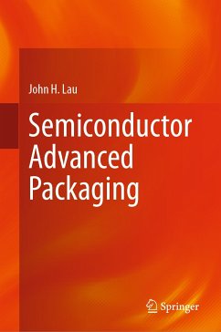
The book focuses on the design, materials, process, fabrication, and reliability of advanced semiconductor packaging components and systems. Both principles and engineering practice have been addressed, with more weight placed on engineering practice. This is achieved by providing in-depth study on a number of major topics such as system-in-package, fan-in wafer/panel-level chip-scale packages, fan-out wafer/panel-level packaging, 2D, 2.1D, 2.3D, 2.5D, and 3D IC integration, chiplets packaging, chip-to-wafer bonding, wafer-to-wafer bonding, hybrid bonding, and dielectric materials for high…mehr

  • Geräte: PC
  • ohne Kopierschutz
  • eBook Hilfe
  • Größe: 44.94MB
Produktbeschreibung
The book focuses on the design, materials, process, fabrication, and reliability of advanced semiconductor packaging components and systems. Both principles and engineering practice have been addressed, with more weight placed on engineering practice. This is achieved by providing in-depth study on a number of major topics such as system-in-package, fan-in wafer/panel-level chip-scale packages, fan-out wafer/panel-level packaging, 2D, 2.1D, 2.3D, 2.5D, and 3D IC integration, chiplets packaging, chip-to-wafer bonding, wafer-to-wafer bonding, hybrid bonding, and dielectric materials for high speed and frequency. The book can benefit researchers, engineers, and graduate students in fields of electrical engineering, mechanical engineering, materials sciences, and industry engineering, etc.

Dieser Download kann aus rechtlichen Gründen nur mit Rechnungsadresse in A, B, BG, CY, CZ, D, DK, EW, E, FIN, F, GR, HR, H, IRL, I, LT, L, LR, M, NL, PL, P, R, S, SLO, SK ausgeliefert werden.

Autorenporträt
John H. Lau, Ph.D., P.E. has been the CTO of Unimicron in Taiwan since August 2019. Prior to that, he was a Senior Technical Advisor at ASM Pacific Technology in Hong Kong for 5 years; a specialist of the Industrial Technology Research Institute in Taiwan for 4¿ years and a Senior Scientist/MTS at Hewlett-Packard Laboratory/Agilent in California for more than 25 years. He earrned a Ph.D. degree in theoretical and applied mechanics from the University of Illinois at Urbana-Champaign.With more than 40 years of R&D and manufacturing experience, he has authored or coauthored more than 480 peer-reviewed technical publications, invented more than 30 issued or pending US patents, and given more than 300 lectures/workshops/keynotes worldwide. He has authored or coauthored 20 textbooks on fan-out wafer-level packaging, 3D IC heterogeneous integration and packaging, TSV for 3D integration, advanced MEMS packaging, reliability of 2D and 3D IC interconnects, flip chip, WLP, MCM, area-array packages, WLCSP, high-density PCB, SMT, DCA, TAB, lead-free materials, soldering, manufacturing, and solder joint reliability.

He has received many awards from the American Society of Mechanical Engineers (ASME), the Institute of Electrical and Electronics Engineers (IEEE), the Society of Manufacturing Engineers (SME) and other societies. He is an elected ASME fellow, IEEE fellow, and IMAPS fellow, and has been heavily involved in many of ASME's, IEEE's, and IMAPS' technical activities.