Jun Ohta
Smart CMOS Image Sensors and Applications (eBook, ePUB)
51,95 €
51,95 €
inkl. MwSt.
Sofort per Download lieferbar

26 °P sammeln
51,95 €
Als Download kaufen

51,95 €
inkl. MwSt.
Sofort per Download lieferbar

26 °P sammeln
Jetzt verschenken
Alle Infos zum eBook verschenken
51,95 €
inkl. MwSt.
Sofort per Download lieferbar
Alle Infos zum eBook verschenken

26 °P sammeln
Jun Ohta
Smart CMOS Image Sensors and Applications (eBook, ePUB)
- Format: ePub
- Merkliste
- Auf die Merkliste
- Bewerten Bewerten
- Teilen
- Produkt teilen
- Produkterinnerung
- Produkterinnerung

Bitte loggen Sie sich zunächst in Ihr Kundenkonto ein oder registrieren Sie sich bei
bücher.de, um das eBook-Abo tolino select nutzen zu können.
Hier können Sie sich einloggen
Hier können Sie sich einloggen
Sie sind bereits eingeloggt. Klicken Sie auf 2. tolino select Abo, um fortzufahren.

Bitte loggen Sie sich zunächst in Ihr Kundenkonto ein oder registrieren Sie sich bei bücher.de, um das eBook-Abo tolino select nutzen zu können.
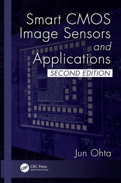
This book provides the state-of-the-art of CMOS image sensors and applications. The book describes the fundamentals of CMOS image sensors, optoelectronic device physics, and introduces typical CMOS image sensor structures, such as an active pixel sensor (APS).
- Geräte: eReader
- mit Kopierschutz
- eBook Hilfe
Andere Kunden interessierten sich auch für
![Smart CMOS Image Sensors and Applications (eBook, PDF) Smart CMOS Image Sensors and Applications (eBook, PDF)]() Jun OhtaSmart CMOS Image Sensors and Applications (eBook, PDF)51,95 €
Jun OhtaSmart CMOS Image Sensors and Applications (eBook, PDF)51,95 €![Multimedia Image and Video Processing (eBook, ePUB) Multimedia Image and Video Processing (eBook, ePUB)]() Multimedia Image and Video Processing (eBook, ePUB)85,95 €
Multimedia Image and Video Processing (eBook, ePUB)85,95 €![Design of Event-Driven SPAD-Based 3D Image Sensors (eBook, ePUB) Design of Event-Driven SPAD-Based 3D Image Sensors (eBook, ePUB)]() Rubén Gómez-MerchánDesign of Event-Driven SPAD-Based 3D Image Sensors (eBook, ePUB)114,95 €
Rubén Gómez-MerchánDesign of Event-Driven SPAD-Based 3D Image Sensors (eBook, ePUB)114,95 €![Microelectronics and Signal Processing (eBook, ePUB) Microelectronics and Signal Processing (eBook, ePUB)]() Microelectronics and Signal Processing (eBook, ePUB)46,95 €
Microelectronics and Signal Processing (eBook, ePUB)46,95 €![Signals and Images (eBook, ePUB) Signals and Images (eBook, ePUB)]() Signals and Images (eBook, ePUB)80,95 €
Signals and Images (eBook, ePUB)80,95 €![Time-Frequency Analysis Techniques and their Applications (eBook, ePUB) Time-Frequency Analysis Techniques and their Applications (eBook, ePUB)]() Ram Bilas PachoriTime-Frequency Analysis Techniques and their Applications (eBook, ePUB)47,95 €
Ram Bilas PachoriTime-Frequency Analysis Techniques and their Applications (eBook, ePUB)47,95 €![Technologies for Smart Sensors and Sensor Fusion (eBook, ePUB) Technologies for Smart Sensors and Sensor Fusion (eBook, ePUB)]() Technologies for Smart Sensors and Sensor Fusion (eBook, ePUB)88,95 €
Technologies for Smart Sensors and Sensor Fusion (eBook, ePUB)88,95 €-
-
-
This book provides the state-of-the-art of CMOS image sensors and applications. The book describes the fundamentals of CMOS image sensors, optoelectronic device physics, and introduces typical CMOS image sensor structures, such as an active pixel sensor (APS).
Hinweis: Dieser Artikel kann nur an eine deutsche Lieferadresse ausgeliefert werden.
Dieser Download kann aus rechtlichen Gründen nur mit Rechnungsadresse in A, B, BG, CY, CZ, D, DK, EW, E, FIN, F, GR, HR, H, IRL, I, LT, L, LR, M, NL, PL, P, R, S, SLO, SK ausgeliefert werden.
Hinweis: Dieser Artikel kann nur an eine deutsche Lieferadresse ausgeliefert werden.
Produktdetails
- Produktdetails
- Verlag: Taylor & Francis eBooks
- Seitenzahl: 309
- Altersempfehlung: ab 12 Jahre
- Erscheinungstermin: 12. Mai 2020
- Englisch
- ISBN-13: 9781351652346
- Artikelnr.: 59436426
- Verlag: Taylor & Francis eBooks
- Seitenzahl: 309
- Altersempfehlung: ab 12 Jahre
- Erscheinungstermin: 12. Mai 2020
- Englisch
- ISBN-13: 9781351652346
- Artikelnr.: 59436426
- Herstellerkennzeichnung Die Herstellerinformationen sind derzeit nicht verfügbar.
Jun Ohta received the B.E., M.E., and Dr. Eng. degrees in applied physics, all from the University of Tokyo, Japan, in 1981, 1983, and 1992, respectively. In 1983, he joined Mitsubishi Electric Corporation, Hyogo, Japan. From 1992 to 1993, he was a visiting scientist in Optoelectronics Computing Systems Center, University of Colorado at Boulder. In 1998, he joined Graduate School of Materials Science, Nara Institute of Science and Technology (NAIST), Nara, Japan as Associate Professor. He was appointed as Professor in 2004. His current research interests are smart CMOS image sensors for biomedical applications and retinal prosthetic devices. He serves as the Distinguished Lecturer of IEEE Solid-State Circuits Society, a section editor of IET Journal of Engineering, an associate editor of IEEE Trans. Biomedical Circuits and Systems, an editor of Japanese Journal of Applied Physic, etc. He also served as technical program committee member of IEEE ISSCC, Symposium on VLSI Circuits, IEEE BioCAS 2018, etc. He organized the IEEE BioCAS 2019 at Nara as one of the general co-chairs. He is a senior member of both IEEE and the IEE Japan, and a fellow member of both the JSAP and the ITE Japan.
1 Introduction. A general overview. 1.2 Brief history of CMOS image sensors
. 1.3 Brief history of smart CMOS image sensors. 1.4 Organization of the
book. 2 Fundamentals of CMOS image sensors. 2.1 Introduction. 2.2
Fundamentals of photo detection. 2.2.1 Absorption coefficient. 2.2.2
Behavior of minority carriers. 2.2.3 Sensitivity and quantum efficiency.
2.3 Photodetectors for smart CMOS image sensors. 2.3.1 pn-junction
photodiode. 2.3.2 Photogate. 2.3.3 Phototransistor. 2.3.4 Avalanche
photodiode. 2.3.5 Photoconductive detector. 2.4 Accumulation mode in PDs..
2.4.1 Potential change in accumulation mode. 2.4.2 Potential description.
2.4.3 Behavior of photo-generated carriers in PD. 2.5 Basic pixel
structures. 2.5.1 Passive pixel sensor. 2.5.2 Active pixel sensor,3T-APS.
2.5.3 Active pixel sensor,4T-APS. 2.6 Sensor peripherals. 2.6.1 Addressing.
2.6.2 Readout circuits. 2.6.3 Analog-to-digital converters. 2.7 Basic
sensor characteristics. 2.7.1 Noise. 2.7.2 Dynamic range. 2.7.3 Speed. 2.8
Color. 2.9 Pixel sharing. 2.10 Comparison between pixel architecture. 2.11
Comparison with CCDs. 3 Smart functions and materials. 3.1 Introduction 3.2
Pixel structure. 3.2.1 Current mode. 3.2.2 Log sensor. 3.3 Analog
operation. 3.3.1 Winner-take-all. 3.3.2 Projection. 3.3.3 Resistive
network. 3.4 Pulse modulation. 3.4.1 Pulse width modulation. 3.4.2 Pulse
frequency modulation. 3.5 Digital processing. 3.6 Materials other than
silicon. 3.6.1 Silicon-on-insulator. 3.6.2 Extending the detection
wavelength. 3.7 Structures other than standard CMOS technologies. 3.7.1 3D
integration. 3.7.2 Integration with light emitters. 3.7.3 Color realization
using nonstandard structures. 4 Smart imaging. 4.1 Introduction. 4.2 Low
light imaging. 4.2.2 PFM for lowlight imaging. 4.2.3 Differential APS.
4.2.4 Geiger mode APD for a smart CMOS image sensor. 4.3 High speed. 4.3.1
Global shutter. 4.4 Wide dynamic range. 4.4.1 Principle of wide dynamic
range. 4.4.2 Dual sensitivity. 4.4.3 Nonlinear response. 4.4.4 Multiple
sampling. 4.4.5 Saturation detection. 4.4.6 Diffusive brightness. 4.5
Demodulation. 4.5.1 Principles of demodulation. 4.5.2 Correlation. 4.5.3
Method of two accumulation regions. 4.6 Three-dimensional rangefinder.
4.6.1 Time of flight. 4.6.2 Triangulation. 4.6.3 Depth key. 4.7 Target
tracking. 4.7.1 Maximum detection for target tracking. 4.7.2 Projection for
target tracking. 4.7.3 Resistive network and other analog processing for
target. Tracking. 4.7.4 Digital processing for target tracking. 4.8
Dedicated arrangement of pixel and optics. 4.8.1 Non-orthogonal
arrangement. 4.8.2 Dedicated optics. 4.8.3 Light field detection. 4.9
Polarization detection. 5 Applications. 5.1 Introduction. 5.2 Information
and communication applications. 5.2.1 Optical ID tag. 5.2.2 Optical
wireless communication. 5.3 Biotechnology applications. 5.3.1 Smart CMOS
image sensor with multi-modal functions. 5.3.2 Smart CMOS image sensor with
ISFET. 5.3.3 Potential imaging combining MEMS technology. 5.3.4 Smart CMOS
sensor for optical and electrochemical imaging. 5.3.5 Fluorescence
detection. 5.4 Medical applications. 5.4.1 Capsule endoscope. 5.4.2 Retinal
prosthesis. A Tables of constants. B Illuminance. C Human eye and CMOS
image sensors. D Fundamental characteristics of MOS capacitors. E
Fundamental characteristics of MOSFET. F Optical format and resolution.
References. Index
