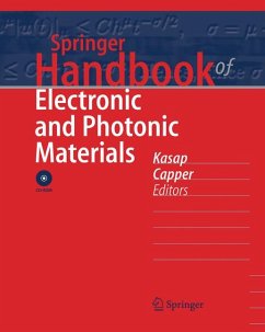
Springer Handbook of Electronic and Photonic Materials / Springer Handbook of Electronic and Photonic Materials (eBook, PDF)
415,31 €
inkl. MwSt.
Sofort per Download lieferbar

0 °P sammeln
Springer Handbook of Electronic and Photonic Materials / Springer Handbook of Electronic and Photonic Materials (eBook, PDF)
- Format: PDF
- Merkliste
- Auf die Merkliste
- Bewerten Bewerten
- Teilen
- Produkt teilen
- Produkterinnerung
- Produkterinnerung

Bitte loggen Sie sich zunächst in Ihr Kundenkonto ein oder registrieren Sie sich bei
bücher.de, um das eBook-Abo tolino select nutzen zu können.
Hier können Sie sich einloggen
Hier können Sie sich einloggen
Sie sind bereits eingeloggt. Klicken Sie auf 2. tolino select Abo, um fortzufahren.

Bitte loggen Sie sich zunächst in Ihr Kundenkonto ein oder registrieren Sie sich bei bücher.de, um das eBook-Abo tolino select nutzen zu können.
Contributions from well known and respected researchers throughout the world Thorough coverage of electronic and opto-electronic materials that today's electrical engineers, material scientists and physicists need Interdisciplinary approach encompasses research in disciplines such as materials science, electrical engineering, chemical engineering, mechanical engineering, physics and chemistry
- Geräte: PC
- ohne Kopierschutz
- eBook Hilfe
- Upload möglich
Andere Kunden interessierten sich auch für
![Digital Transmission Systems (eBook, PDF) Digital Transmission Systems (eBook, PDF)]() David R. SmithDigital Transmission Systems (eBook, PDF)177,95 €
David R. SmithDigital Transmission Systems (eBook, PDF)177,95 €![Introduction to Infrared and Electro-Optical Systems, Second Edition (eBook, PDF) Introduction to Infrared and Electro-Optical Systems, Second Edition (eBook, PDF)]() Ronald G DriggersIntroduction to Infrared and Electro-Optical Systems, Second Edition (eBook, PDF)122,95 €
Ronald G DriggersIntroduction to Infrared and Electro-Optical Systems, Second Edition (eBook, PDF)122,95 €![Systems Approach to Lithium-Ion Battery Management (eBook, PDF) Systems Approach to Lithium-Ion Battery Management (eBook, PDF)]() Phil WeickerSystems Approach to Lithium-Ion Battery Management (eBook, PDF)93,95 €
Phil WeickerSystems Approach to Lithium-Ion Battery Management (eBook, PDF)93,95 €![Photonics (eBook, PDF) Photonics (eBook, PDF)]() Vittorio DegiorgioPhotonics (eBook, PDF)47,59 €
Vittorio DegiorgioPhotonics (eBook, PDF)47,59 €![Springer Handbook of Power Systems (eBook, PDF) Springer Handbook of Power Systems (eBook, PDF)]() Springer Handbook of Power Systems (eBook, PDF)258,95 €
Springer Handbook of Power Systems (eBook, PDF)258,95 €![Passive Components for Dense Optical Integration (eBook, PDF) Passive Components for Dense Optical Integration (eBook, PDF)]() Christina ManolatouPassive Components for Dense Optical Integration (eBook, PDF)73,95 €
Christina ManolatouPassive Components for Dense Optical Integration (eBook, PDF)73,95 €![Electronic Properties of Materials (eBook, PDF) Electronic Properties of Materials (eBook, PDF)]() Rolf E. HummelElectronic Properties of Materials (eBook, PDF)65,95 €
Rolf E. HummelElectronic Properties of Materials (eBook, PDF)65,95 €-
-
-
Contributions from well known and respected researchers throughout the world Thorough coverage of electronic and opto-electronic materials that today's electrical engineers, material scientists and physicists need Interdisciplinary approach encompasses research in disciplines such as materials science, electrical engineering, chemical engineering, mechanical engineering, physics and chemistry
Produktdetails
- Produktdetails
- Verlag: Springer / Springer US
- Erscheinungstermin: 1. August 2007
- Englisch
- ISBN-13: 9780387291857
- Artikelnr.: 58489114
- Verlag: Springer / Springer US
- Erscheinungstermin: 1. August 2007
- Englisch
- ISBN-13: 9780387291857
- Artikelnr.: 58489114
- Herstellerkennzeichnung Die Herstellerinformationen sind derzeit nicht verfügbar.
Safa Kasap is currently a Professor and Canada Research Chair in Electronic Materials and Devices in the Electrical Engineering Department at the University of Saskatchewan, Canada. He obtained his BSc (1976), MSc (1978) and PhD (1983) degrees from the Imperial College of Science, Technology and Medicine, University of London, specializing in amorphous semiconductors and chalcogenide glasses. In 1996 he was awarded the DSc (Engineering) from London University for his research contributions to materials science in electrical engineering. He is a Fellow of the Institution of Electrical Engineers, the Institute of Physics and the Institute of Materials. His research interests are in amorphous semiconductors, glasses for photonics, photoconductors, electrical, optical and thermal properties of materials, and related topics, with more than one hundred refereed journal papers in these areas. He is the Deputy Editor of the Journal of Materials Science: Materials in Electronics (Springer), and a Series Editor for the Series on Materials in Electronic and Optoelectronics (Wiley). Peter Capper has worked for the same company (through several name changes) for over 30 years in the area of II-VI compounds for infrared applications, latterly as a Materials Team Leader in charge of group of scientists working on the growth and characterisation of these compounds. This has been mainly in the area of cadmium mercury telluride and cadmium telluride, the premier infrared materials, by a range of bulk and epitaxial techniques. He has given several invited talks in Japan, USA and Europe, has coauthored over 100 Journal papers, holds one patent and has edited/written 5 books in the field since 1987. He is on the Editorial Board of the J. Mater. Sci.: Mater. Electron. (Springer) and is a Series Editor for Wiley on Materials for Electronics and Optoelectronics.
Each chapter has a concise summary that provides a general overview of the subject in the chapter in a clear language. The chapters begin at fundamentals and build up towards advanced concepts and applications. Emphasis is on physical concepts rather than extensive mathematical derivations. Each chapter is full of clear color illustrations that convey the concepts and make the subject matter enjoyable to read and understand. Examples in the chapters have practical applications. Chapters also have numerous extremely useful tables that summarize equations, experimental techniques, and most importantly, properties of various materials. The chapters have been divided into five parts. Each part has chapters that form a coherent treatment of a given area. Chap. 1 Introduction: Perspectives on Electronic, Optoelectronic, and Photonic MaterialsPart A: Fundamental Electronic, Optical, and Magnetic Properties Part A contains chapters starting from basic concepts and build up to up-to-date knowledge in a logical easy to follow sequence. Part A would be equivalent to a graduate level treatise that starts from basic structural properties to go onto electrical, dielectric, optical, and magnetic properties. Each chapter starts by assuming someone who has completed a degree in physics, chemistry, engineering, or materials science. Chap. 2 Electrical Conduction in Metals and Semiconductors.- Chap. 3 Optical Properties: Fundamentals and Characterization.- Chap. 4 Magnetic Properties.- Chap. 5 Defects in Monocrystalline Silicon.- Chap. 6 Diffusion in Semiconductors.- Chap. 7 Photoconductivity in Materials Research.- Chap. 8 Electronic Properties of Semiconductor Interfaces.- Chap. 9 Description of Charge Transport in Disordered Materials.- Chap. 10 Dielectric Response -- An Overview.- Chap. 11 Ionic Conduction and ApplicationsPart B: Growth and Characterization Part B provides a clear overview of bulk and single-crystal growth, growth techniques (epitaxial crystal growth: LPE, MOVPE, MBE), and the structural, chemical, electrical and thermal characterization of materials. Silicon and II – VI compounds and semiconductors are especially emphasized. Chap. 12 Bulk Crystal Growth.- Chap. 13 Single Crystal Silicon: Growth and Properties.- Chap. 14 Epitaxial Crystal Growth: LPE, MOVPE, MBE.- Chap. 15 II – VI Compounds: Growth.- Chap. 16 Wide Bandgap II – VI Semiconductors: Growth and Properties.- Chap. 17 Structural Characterization.- Chap. 18 Chemical Analysis.- Chap. 19 Thermal Properties and Characterization.- Chap. 20 Electrical Characterization of Semiconductor Materials and DevicesPart C: Materials for Electronics Part C covers specific materials such as crystalline Si, microcrystalline Si, GaAs, high-temperature semiconductors, amorphous semiconductors, ferroelectric materials, and thin and thick films. Chap. 21 Single Crystal Silicon.- Chap. 22 Silicon/Germanium.- Chap. 23 Gallium Arsenide.- Chap. 24 High Temperature Electronic Materials: Silicon Carbide and Diamond.- Chap. 25 Amorphous Semiconductors.- Chap. 26 Amorphous and Microcrystalline Silicon - Preparation and Properties for Devices.- Chap. 27 Ferroelectric Materials.- Chap. 28 Dielectric Materials for Microelectronics.- Chap. 29 Thin Films.- Chap. 30 Thick FilmsPart D: Materials for Optoelectronics and Photonics Part D examines materials that have applications in optoelectronics and photonics. It covers some of the state-of-the-art developments in optoelectronic materials, and covers III – V Ternaries, III-Nitrides, II – VI compounds, quantum wells, photonic crystals, glasses for photonics, nonlinear photonic glasses, nonlinear organic, and luminescent materials. Chap. 31 III – V Ternary and Quaternary Compounds.- Chap. 32 Group III Nitrides.- Chap. 33 Electron Transport Within the III – V Nitride Semiconductors, GaN, AlN, and InN: A Monte Carlo Analysis.- Chap. 34 Cd-based wide bandgap compounds.- Chap. 35 Doping Aspects of Zn-Based Wide Bandgap Semiconductors.- Chap. 36 II – VI Narrow Bandgap Semiconductors: Optoelectronics.- Chap. 37 Optoelectronic Devices and Materials.- Chap. 38 Liquid Crystals.- Chap. 39 Organic Photoconductors.- Chap. 40 Luminescent Materials.- Chap. 41 Nanoengineered Tunable Photonic Crystals in the Near-IR and Visible.- Chap. 42 Quantum Wells, Superlattices and Bandgap Engineering.- Chap. 43 Glasses for Photonic Integration.- Chap. 44 Optical Nonlinearity in Photonic Glasses.- Chap. 45 Nonlinear Optoelectronic MaterialsPart E: Novel Materials and Selected Applications Part E provides a survey on novel materials and applications such as information recording devices (CD, video, DVD) as well as phase-change optical recording. The chapters also include applications such as solar cells, sensors, photoconductors, and carbon nanotubes. Both ends of the spectrum from research to applications are represented in chapters on molecular electronics and packaging materials. Chap. 46 Solar Cells and Photovoltaics.- Chap. 47 Silicon on Mechanically Flexible Substrates for Large Area Electronics.- Chap. 48 Photoconductors for X-ray Image Detectors.- Chap. 49 Phase-change Optical Recording.- Chap. 50 Carbon Nanotubes and Bucky Materials.- Chap. 51 Magnetic Information Storage Materials.- Chap. 52 High-Temperature Superconductors.- Chap. 53 Molecular Electronics.- Chap. 54 Organic Materials for Chemical Sensing.- Chap. 55 Packaging Materials Glossary of Terms About the Authors Subject Index
Each chapter has a concise summary that provides a general overview of the subject in the chapter in a clear language. The chapters begin at fundamentals and build up towards advanced concepts and applications. Emphasis is on physical concepts rather than extensive mathematical derivations. Each chapter is full of clear color illustrations that convey the concepts and make the subject matter enjoyable to read and understand. Examples in the chapters have practical applications. Chapters also have numerous extremely useful tables that summarize equations, experimental techniques, and most importantly, properties of various materials. The chapters have been divided into five parts. Each part has chapters that form a coherent treatment of a given area. Chap. 1 Introduction: Perspectives on Electronic, Optoelectronic, and Photonic MaterialsPart A: Fundamental Electronic, Optical, and Magnetic Properties Part A contains chapters starting from basic concepts and build up to up-to-date knowledge in a logical easy to follow sequence. Part A would be equivalent to a graduate level treatise that starts from basic structural properties to go onto electrical, dielectric, optical, and magnetic properties. Each chapter starts by assuming someone who has completed a degree in physics, chemistry, engineering, or materials science. Chap. 2 Electrical Conduction in Metals and Semiconductors.- Chap. 3 Optical Properties: Fundamentals and Characterization.- Chap. 4 Magnetic Properties.- Chap. 5 Defects in Monocrystalline Silicon.- Chap. 6 Diffusion in Semiconductors.- Chap. 7 Photoconductivity in Materials Research.- Chap. 8 Electronic Properties of Semiconductor Interfaces.- Chap. 9 Description of Charge Transport in Disordered Materials.- Chap. 10 Dielectric Response -- An Overview.- Chap. 11 Ionic Conduction and ApplicationsPart B: Growth and Characterization Part B provides a clear overview of bulk and single-crystal growth, growth techniques (epitaxial crystal growth: LPE, MOVPE, MBE), and the structural, chemical, electrical and thermal characterization of materials. Silicon and II – VI compounds and semiconductors are especially emphasized. Chap. 12 Bulk Crystal Growth.- Chap. 13 Single Crystal Silicon: Growth and Properties.- Chap. 14 Epitaxial Crystal Growth: LPE, MOVPE, MBE.- Chap. 15 II – VI Compounds: Growth.- Chap. 16 Wide Bandgap II – VI Semiconductors: Growth and Properties.- Chap. 17 Structural Characterization.- Chap. 18 Chemical Analysis.- Chap. 19 Thermal Properties and Characterization.- Chap. 20 Electrical Characterization of Semiconductor Materials and DevicesPart C: Materials for Electronics Part C covers specific materials such as crystalline Si, microcrystalline Si, GaAs, high-temperature semiconductors, amorphous semiconductors, ferroelectric materials, and thin and thick films. Chap. 21 Single Crystal Silicon.- Chap. 22 Silicon/Germanium.- Chap. 23 Gallium Arsenide.- Chap. 24 High Temperature Electronic Materials: Silicon Carbide and Diamond.- Chap. 25 Amorphous Semiconductors.- Chap. 26 Amorphous and Microcrystalline Silicon - Preparation and Properties for Devices.- Chap. 27 Ferroelectric Materials.- Chap. 28 Dielectric Materials for Microelectronics.- Chap. 29 Thin Films.- Chap. 30 Thick FilmsPart D: Materials for Optoelectronics and Photonics Part D examines materials that have applications in optoelectronics and photonics. It covers some of the state-of-the-art developments in optoelectronic materials, and covers III – V Ternaries, III-Nitrides, II – VI compounds, quantum wells, photonic crystals, glasses for photonics, nonlinear photonic glasses, nonlinear organic, and luminescent materials. Chap. 31 III – V Ternary and Quaternary Compounds.- Chap. 32 Group III Nitrides.- Chap. 33 Electron Transport Within the III – V Nitride Semiconductors, GaN, AlN, and InN: A Monte Carlo Analysis.- Chap. 34 Cd-based wide bandgap compounds.- Chap. 35 Doping Aspects of Zn-Based Wide Bandgap Semiconductors.- Chap. 36 II – VI Narrow Bandgap Semiconductors: Optoelectronics.- Chap. 37 Optoelectronic Devices and Materials.- Chap. 38 Liquid Crystals.- Chap. 39 Organic Photoconductors.- Chap. 40 Luminescent Materials.- Chap. 41 Nanoengineered Tunable Photonic Crystals in the Near-IR and Visible.- Chap. 42 Quantum Wells, Superlattices and Bandgap Engineering.- Chap. 43 Glasses for Photonic Integration.- Chap. 44 Optical Nonlinearity in Photonic Glasses.- Chap. 45 Nonlinear Optoelectronic MaterialsPart E: Novel Materials and Selected Applications Part E provides a survey on novel materials and applications such as information recording devices (CD, video, DVD) as well as phase-change optical recording. The chapters also include applications such as solar cells, sensors, photoconductors, and carbon nanotubes. Both ends of the spectrum from research to applications are represented in chapters on molecular electronics and packaging materials. Chap. 46 Solar Cells and Photovoltaics.- Chap. 47 Silicon on Mechanically Flexible Substrates for Large Area Electronics.- Chap. 48 Photoconductors for X-ray Image Detectors.- Chap. 49 Phase-change Optical Recording.- Chap. 50 Carbon Nanotubes and Bucky Materials.- Chap. 51 Magnetic Information Storage Materials.- Chap. 52 High-Temperature Superconductors.- Chap. 53 Molecular Electronics.- Chap. 54 Organic Materials for Chemical Sensing.- Chap. 55 Packaging Materials Glossary of Terms About the Authors Subject Index
