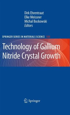
Technology of Gallium Nitride Crystal Growth (eBook, PDF)
157,95 €
inkl. MwSt.
Sofort per Download lieferbar
Technology of Gallium Nitride Crystal Growth (eBook, PDF)
- Format: PDF
- Merkliste
- Auf die Merkliste
- Bewerten Bewerten
- Teilen
- Produkt teilen
- Produkterinnerung
- Produkterinnerung
Bitte loggen Sie sich zunächst in Ihr Kundenkonto ein oder registrieren Sie sich bei
bücher.de, um das eBook-Abo tolino select nutzen zu können.
Hier können Sie sich einloggen
Sie sind bereits eingeloggt. Klicken Sie auf 2. tolino select Abo, um fortzufahren.
Bitte loggen Sie sich zunächst in Ihr Kundenkonto ein oder registrieren Sie sich bei bücher.de, um das eBook-Abo tolino select nutzen zu können.
- Geräte: PC
- ohne Kopierschutz
- eBook Hilfe
- Größe: 10.73MB
- Upload möglich
Andere Kunden interessierten sich auch für
- Dinker B. SirdeshmukhAtomistic Properties of Solids (eBook, PDF)110,95 €
- Mikhail KorzhikPhysics of Fast Processes in Scintillators (eBook, PDF)160,49 €
- Piezoelectricity (eBook, PDF)157,95 €
- Vladimir G. DubrovskiiNucleation Theory and Growth of Nanostructures (eBook, PDF)134,95 €
- Introduction to the Physics of Diluted Magnetic Semiconductors (eBook, PDF)110,95 €
- Michael LeitnerStudying Atomic Dynamics with Coherent X-rays (eBook, PDF)39,95 €
- Paolo OssiDisordered Materials (eBook, PDF)71,95 €
-
-
-
Produktdetails
- Verlag: Springer Berlin
- Erscheinungstermin: 14. Juni 2010
- Englisch
- ISBN-13: 9783642048302
- Artikelnr.: 37365644
Dr. Dirk Ehrentraut received a Diploma in Crystallography from the Humboldt University of Berlin, Germany and a Ph.D. in Sciences from the Institute of Applied Optics at the Swiss Federal Institute of Technology in Lausanne (EPFL), Switzerland. He joined the Tohoku University end of 2003 and is currently a visiting professor of the Institute of Multidisciplinary Research of Advanced Materials. His field of competence covers the crystal growth of films and bulk material from the liquid and vapor phase and material aspects of the wide band gap semiconductors of group-III nitrides and ZnO. He has authored 130 publications in books, journals and conferences and holds 6 patents.
Dr. Elke Meissner graduated from the University of Erlangen, Germany in the field of applied mineralogy. Later she received a PhD from the University of Bayreuth, Germany. She is a senior scientist in the Department of Crystal Growth at the Fraunhofer Institute of Integrated Systems and Device Technology (IISB) in Erlangen and became head of the working group Defect Engineering in 2007. She has a broad background in process properties correlation for advanced materials in various fields like silicon nitride ceramics and applied & experimental mineralogy. Her recent work is strongly focussed on the structural characterization of crystals and crystal layers of novel semiconductors. Dr. Meissner is inventor or co-inventor of 3 international patents and authored more than 50 papers or contributions to journals and conference.
Dr. Michal Bockowski received the M.Sc. Eng. in Solid State Physics from the Warsaw University of Technology, Poland and the Ph.D. in the Chemistry of Solids 1995 from the University Montpellier II, France. He is currently a Research Associate of the Institute of High Pressure Physics of the Polish Academy of Sciences and a technologist at TopGaN Ltd., Poland. He has authored >120 publications in journals and conferences and holds 2 international patents.
Market for Bulk GaN Crystals.- Development of the Bulk GaN Substrate Market.- Vapor Phase Growth Technology.- Hydride Vapor Phase Epitaxy of GaN.- Growth of Bulk GaN Crystals by HVPE on Single Crystalline GaN Seeds.- Freestanding GaN Wafers by Hydride Vapor Phase Epitaxy Using Void-Assisted Separation Technology.- Nonpolar and Semipolar GaN Growth by HVPE.- High Growth Rate MOVPE.- Solution Growth Technology.- Ammonothermal Growth of GaN Under Ammono-Basic Conditions.- A Pathway Toward Bulk Growth of GaN by the Ammonothermal Method.- Acidic Ammonothermal Growth Technology for GaN.- Flux Growth Technology.- High Pressure Solution Growth of Gallium Nitride.- A Brief Review on the Na-Flux Method Toward Growth of Large-Size GaN Crystal.- Low Pressure Solution Growth of Gallium Nitride.- Characterization of GaN Crystals.- Optical Properties of GaN Substrates.- Point Defects and Impurities in Bulk GaN Studied by Positron Annihilation Spectroscopy.
Preface.- Development of the Gallium Nitride Market.- HVPE of GaN.- Growth of Bulk GaN Crystals by HVPE on Single Crystalline GaN Seeds.- HVPE at Hitachi Cable.- HVPE Technology.- High-Growth Rate MOCVD.- Ammonothermal Solution Growth.- High-Pressure Solution (HPS) Growth of Gallium Nitride.- Na Flux LPE.- Ga Flux LPE.- Optical Properties of GaN Substrates.- Structural Properties of GaN.