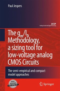
The gm/ID Methodology, a sizing tool for low-voltage analog CMOS Circuits (eBook, PDF)
The semi-empirical and compact model approaches
Versandkostenfrei!
Sofort per Download lieferbar
96,95 €
inkl. MwSt.
Weitere Ausgaben:

PAYBACK Punkte
48 °P sammeln!
This book provides a comprehensive overview of design methodologies for Analog Circuits, and includes a MATLAB dedicated toolbox. The MATLAB toolbox offers the possibility of performing virtual hands-on experiments related to MOS transistor physics as well as finding currents and transistor sizes for well-known CMOS circuits. The book's objective is to suggest straightforward methodologies at the earliest possible design stage and find currents and sizes very close to optimality. The methodology takes advantage of compact MOS models while following classical design procedures. This is also the...
This book provides a comprehensive overview of design methodologies for Analog Circuits, and includes a MATLAB dedicated toolbox. The MATLAB toolbox offers the possibility of performing virtual hands-on experiments related to MOS transistor physics as well as finding currents and transistor sizes for well-known CMOS circuits. The book's objective is to suggest straightforward methodologies at the earliest possible design stage and find currents and sizes very close to optimality. The methodology takes advantage of compact MOS models while following classical design procedures. This is also the first 'book' to present the gm/ID synthesis methodology to which an increasing number of papers refer. Finally, the users' guide, described in the annex, should enable the reader to run their own tests.
Dieser Download kann aus rechtlichen Gründen nur mit Rechnungsadresse in A, B, BG, CY, CZ, D, DK, EW, E, FIN, F, GR, HR, H, IRL, I, LT, L, LR, M, NL, PL, P, R, S, SLO, SK ausgeliefert werden.


