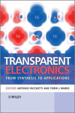
Transparent Oxide Electronics (eBook, PDF)
From Materials to Devices
Alle Infos zum eBook verschenken
Transparent Oxide Electronics (eBook, PDF)
From Materials to Devices
- Format: PDF
- Merkliste
- Auf die Merkliste
- Bewerten Bewerten
- Teilen
- Produkt teilen
- Produkterinnerung
- Produkterinnerung
Hier können Sie sich einloggen
Bitte loggen Sie sich zunächst in Ihr Kundenkonto ein oder registrieren Sie sich bei bücher.de, um das eBook-Abo tolino select nutzen zu können.
Transparent electronics is emerging as one of the most promising technologies for the next generation of electronic products, away from the traditional silicon technology. It is essential for touch display panels, solar cells, LEDs and antistatic coatings. The book describes the concept of transparent electronics, passive and active oxide semiconductors, multicomponent dielectrics and their importance for a new era of novel electronic materials and products. This is followed by a short history of transistors, and how oxides have revolutionized this field. It concludes with a glance at…mehr
- Geräte: PC
- mit Kopierschutz
- eBook Hilfe
- Größe: 30.68MB
- Charge Transport in Disordered Solids with Applications in Electronics (eBook, PDF)228,99 €
- Pedro BarquinhaTransparent Oxide Electronics (eBook, ePUB)121,99 €
- Crystal Growth Processes Based on Capillarity (eBook, PDF)182,99 €
- Rainer WeschePhysical Properties of High-Temperature Superconductors (eBook, PDF)139,99 €
- Adrian KitaiPrinciples of Solar Cells, LEDs and Related Devices (eBook, PDF)75,99 €
- Yuan-Hua LinOxide Thermoelectric Materials (eBook, PDF)124,99 €
- Transparent Electronics (eBook, PDF)159,99 €
-
-
-
Dieser Download kann aus rechtlichen Gründen nur mit Rechnungsadresse in A, B, BG, CY, CZ, D, DK, EW, E, FIN, F, GR, HR, H, IRL, I, LT, L, LR, M, NL, PL, P, R, S, SLO, SK ausgeliefert werden.
- Produktdetails
- Verlag: Jossey-Bass
- Seitenzahl: 360
- Erscheinungstermin: 15. März 2012
- Englisch
- ISBN-13: 9781119967002
- Artikelnr.: 37349496
- Verlag: Jossey-Bass
- Seitenzahl: 360
- Erscheinungstermin: 15. März 2012
- Englisch
- ISBN-13: 9781119967002
- Artikelnr.: 37349496
- Herstellerkennzeichnung Die Herstellerinformationen sind derzeit nicht verfügbar.
Acknowledgments xv
1 Introduction 1
1.1 Oxides and Transparent Electronics: Fundamental Research or Heading
Towards Commercial Products? 1
1.2 The Need for Transparent (Semi)Conductors 3
1.3 Reaching Full Transparency: Dielectrics and Substrates 5
References 6
2 N-type Transparent Semiconducting Oxides 9
2.1 Introduction: Binary and Multicomponent Oxides 9
2.1.1 Binary Compounds: the Examples of Zinc Oxide and Indium Oxide 9
2.1.2 Ternary and Quaternary Compounds: the Examples of Indium-Zinc Oxide
and Gallium-Indium-Zinc Oxide 12
2.2 Sputtered n-TSOs: Gallium-Indium-Zinc Oxide System 16
2.2.1 Dependence of the Growth Rate on Oxygen Content in the Ar+O2 Mixture
and Target Composition 16
2.2.2 Structural and Morphological Properties 18
2.2.3 Electrical Properties 22
2.2.4 Optical Properties 41
2.3 Sputtered n-TSOs: Gallium-Zinc-Tin Oxide System 49
2.4 Solution-Processed n-TSOs 51
2.4.1 ZTO by Spray-pyrolysis 51
2.4.2 ZTO by Sol-gel Spin-coating 52
2.4.3 GIZO Sol-gel by Spin-coating 52
References 55
3 P-type Transparent Conductors and Semiconductors 63
3.1 Introduction 63
3.2 P-type Transparent Conductive Oxides 64
3.3 Thin Film Copper Oxide Semiconductors 66
3.3.1 Role of Oxygen in the Structure, Electrical and Optical Performance
70
3.4 Thin Film Tin Oxide Semiconductors 75
3.4.1 Structure, Composition and Morphology of Tin Oxide Films 78
3.4.2 Electrical and Optical Properties of Tin Oxide Films 84
References 94
4 Gate Dielectrics in Oxide Electronics 101
4.1 Introduction 101
4.2 High-k Dielectrics: Why Not? 102
4.3 Requirements 103
4.4 High-k Dielectrics Deposition 106
4.5 Sputtered High-k Dielectrics in Oxide TFTs 106
4.6 Hafnium Oxide 107
4.6.1 Multicomponent Co-sputtered HfO2 Based Dielectrics 117
4.6.2 Multicomponent Dielectrics from Single Target 126
4.7 Tantalum Oxide (Ta2O5) 130
4.7.1 Multicomponent Ta2O5 Based Dielectrics 133
4.8 Multilayer Dielectrics 138
4.9 High-k Dielectrics/Oxide Semiconductors Interface 141
4.10 Summary 146
References 147
5 The (R)evolution of Thin-Film Transistors (TFTs) 155
5.1 Introduction: Device Operation, History and Main Semiconductor
Technologies 155
5.1.1 Device Structure and Operation 155
5.1.2 Brief History of TFTs 161
5.1.3 Comparative Overview of Dominant TFT Technologies 168
5.2 Fabrication and Characterization of Oxide TFTs 170
5.2.1 N-type GIZO TFTs by Physical Vapor Deposition 171
5.2.2 N-type GZTO TFTs by Physical Vapor Deposition 187
5.2.3 N-type Oxide TFTs by Solution Processing 189
5.2.4 P-type Oxide TFTs by Physical Vapor Deposition 193
5.2.5 N-type GIZO TFTs with Sputtered Dielectrics 196
References 202
6 Electronics With and On Paper 211
6.1 Introduction 211
6.2 Paper in Electronics 212
6.3 Paper Properties 214
6.3.1 Structure, Morphology and Thermal Properties 214
6.3.2 Electrical Properties of the Paper 218
6.4 Resistivity Behaviour of Transparent Conductive Oxides Deposited on
Paper 223
6.5 Paper Transistors 225
6.5.1 Current Transport in Paper Transistors 228
6.6 Floating Gate Non-volatile Paper Memory Transistor 230
6.6.1 Memory Paper Device Feasibility and Stability 233
6.6.2 Memory Selective and Charge Retention Time Behaviors 234
6.7 Complementary Metal Oxide Semiconductor Circuits With and On Paper -
Paper CMOS 237
6.7.1 Capacitance-Voltage and Current-Voltage Characteristics of N/P-Type
Paper Transistors 240
6.7.2 N- and P-channel Paper FET Operation 243
6.7.3 CMOS Inverter Working Principles 244
6.7.4 Paper CMOS Performance 246
6.8 Solid State Paper Batteries 249
6.9 Electrochromic Paper Transistors 252
6.10 Paper UV Light Sensors 255
References 256
7 A Glance at Current and Upcoming Applications 267
7.1 Introduction: Emerging Areas for (Non-)transparent Electronics Based on
Oxide Semiconductors 267
7.2 Active Matrices for Displays 268
7.2.1 Display Market Overview and Future Trends 268
7.2.2 Driving Schemes and TFT Requirements for LCD and OLED Displays 269
7.2.3 Displays with Oxide-Based Backplanes 271
7.3 Transparent Circuits 273
7.3.1 Inverters and Ring Oscillators 273
7.3.2 The Introduction of Oxide CMOS 275
7.4 Oxide Semiconductor Heterojunctions 278
7.4.1 Oxide Semiconductor Heterojunctions in the Literature 278
7.4.2 GIZO Heterojunctions Fabricated at CENIMAT 279
7.5 Field Effect Biosensors 280
7.5.1 Device Types and Working Principles 280
7.5.2 Oxide-Based Biosensors Fabricated at CENIMAT 281
References 284
Index 287