Plasmonics is a large part of the field of nanophotonics. Besides a wide range
of industrial applications already developed, e.g. enhanced biosensors and diodes,
surface plasmon polaritons (SPPs) are still an expanding field of research.
In conventional optics, working on the sub-wavelength scale is not trivial, and
structures smaller than half the wavelength will not lead to results expected by
traditional optics. State-of-the-art microchips and optical data storage devices are
fabricated at the limit of conventional optics. SPPs could open up the way to
sub-wavelength optics far beyond the diffraction limit as demonstrated by Ebbesen
in 1998. The length scales for SPPs span over seven orders of magnitude, from
several nanometers, the penetration depth into metal, to several centimeters, the
propagation length of long range plasmons, making them very interesting objects
for investigation.
The subject of this thesis is the investigation on dielectric loaded surface plasmon
polariton waveguides (DLSPPWs). DLSPPWs are theoretically analysed by computational
simulations at telecommunication wavelength at 1550nm. The waveguides
are experimentally examined using leakage radiation microscopy for 632nm
and 800nm wavelength. The experimental results are compared with simulation
results of corresponding wavelengths. Furthermore, SPP structures like bends and
Y-splitters are investigated. A novel cut-splitter design for an SPP Y-splitter is
introduced and compared to existing designs. For the cut-splitter an improved efficiency
and a better tolerance against fabrication imperfections due to limited resolution
than for conventional Y-splitter designs is demonstrated through experimental
investigations and simulations.
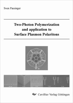
For the fabrication of DLSPPWs, 2-Photon Polymerization (2PP) is, because of
its high flexibility and low costs compared to other nanostructuring technologies,
and easy adaptability. Since the first publication about 2-Photon-Polymerization
by S. Kawata in 1997, the interest and research in this technology has been continuously
increasing. Progress in this technique has been mainly initiated by scientific
interest for use as a rapid prototyping technology. To transfer the 2PP technology
to industrial applications, a novel structuring system is developed and set up during
this work. The 2PP writing speed is increased by a factor of about 100, compared to
results in other publications. Three-dimensional structures with resolutions smaller
than 300nm are reproducible fabricated with writing speeds of about 30mm/s.
Dieser Download kann aus rechtlichen Gründen nur mit Rechnungsadresse in A, B, BG, CY, CZ, D, DK, EW, E, FIN, F, GR, HR, H, IRL, I, LT, L, LR, M, NL, PL, P, R, S, SLO, SK ausgeliefert werden.
Hinweis: Dieser Artikel kann nur an eine deutsche Lieferadresse ausgeliefert werden.


