Decreasing the size of transistor structures (“scaling”') is an ongoing trend in microelectronics, since smaller structures allow more chips to be placed on a wafer. So far, the result has always been a cost saving, with increasing complexity and clock frequency as welcome side effects. But shrinking the conventional MOSFET, on which the conventional CMOS technology is built on, leads to an increasing number of problems with every new technology generation. Many electrical parameters of the conventional MOSFET deteriorate by shrinking its channel length. The resulting short channel effects require ever more complicated compensation structures. Yet certain parameters such as the sub-threshold swing or the width of space charge regions do not scale. Thus, with decreasing channel length it becomes increasingly difficult to design a conventional MOSFET that can be switched off. Approaching approximately 10 nm, electrons would tunnel through the channel region even if the device was to be turned off, leading to unacceptable leakage currents.
Instead of trying to avoid quantum mechanical tunneling, we could try to take advantage of it. This leads to the concept of the tunnel FET. It consists of a p-i-n diode, which has to be reverse-biased, and a gate stack like a conventional MOSFET. Its off-current is the leakage current of the p-i-n diode, which is extremely low and caused mainly by charge carrier generation in the intrinsic region. A positive gate voltage creates an electron-channel at the surface of the intrinsic region, which leads to a strong band bending at the p-end of the device. This allows electrons to tunnel from the valence band to the conduction band, resulting in a tunneling current. The same happens between the n-end of the device and a hole-channel caused by a negative gate voltage.
The motivation for this work is the fact that this device concept of the tunnel FET has already been studied by different groups by means of computer simulations, which already improved the physical understanding of this novel concept. In addition, experimental prototypes have also been produced. However, their doping profiles do not meet the stringent demands, which have to be fulfilled in order to utilize the full potential of this device concept. Conventional CMOS technologies are insufficient, because the tunnel FET needs extremely sharp doping profiles, meaning very high concentration gradients. This is why the electrical characteristics of experimental prototypes have so far deviated significantly from computer simulations.
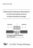
This work focuses on the development of manufacturing processes for experimental prototypes, which show the required doping profiles. The main idea is to realize the tunnel FET vertically. First, the p-i-n layer stack was grown by epitaxy on a silicon substrate. Then freestanding mesa structures were created, by etching away all unnecessary parts of the p-i-n stack. This was followed by a gate stack; a passivation layer; and metal contacts. This method is already known from earlier work and is not applicable for mass production, but it has the important advantage that the channel length is determined by the epitaxy and can be controlled on a nanometer scale, despite the use of cheap photo lithography with a large minimum feature size.
A serious problem of earlier investigations was the etching of the mesa structures; the achieved surface quality did not allow thin gate oxides. This resulted in a higher thermal budget, which led to a high diffusion of the doping atoms.
Therefore a central aspect of this new work is: the development of a special dry-etch process for the necessary surface quality; the improvement of existing process steps; and the integration of new process modules into the device. In addition, the development of this process technology facilitated the production of SiGe tunnel FETs for the first time.
The vertical transistor technology has been optimized to such an extent, that gate oxide thicknesses of less than 4 nm could be used and high surface mobilities could be achieved. This also revealed the limits of the vertical concept. Due to the high band gap of silicon, tunnel FETs made in silicon show an on-current which is far below industrial requirements. Any dopant diffusion reduces the on-current further. Simulations predict that the means of solving this problem could be the introduction of SiGe into the device, which is also a vital part of this work. However, this complicated the production of the gate stack for the vertical transistors, because the gate dielectric could not be grown by thermal oxidation and had to be replaced by an LPCVD silicon nitride
The experimental prototypes built for this work confirmed most of the properties of the tunnel FET, which had been predicted by simulations. The drain current depends exponentially on the gate voltage. The spot-swing (a parameter similar to the subthreshold swing of a conventional MOSFET) depends on the gate voltage but not on temperature, and thus could be theoretically less than 60 mV/dec. The leakage currents are several orders of magnitudes below the ITRS requirements, and the output characteristics show perfect saturation independent of gate length. Since it is almost independent of temperature, the tunnel FET can be used above 120 °C with only minor changes of the electrical parameters, and thus at conditions which render the conventional MOSFET inoperable. The results obtained from the SiGe devices indicate that the on-current can be raised by orders of magnitude by using SiGe, as shown in simulations. However, further experiments will be necessary before any reliable conclusions can be drawn.
Dieser Download kann aus rechtlichen Gründen nur mit Rechnungsadresse in A, B, BG, CY, CZ, D, DK, EW, E, FIN, F, GR, HR, H, IRL, I, LT, L, LR, M, NL, PL, P, R, S, SLO, SK ausgeliefert werden.


